SLVSEN8B July 2018 – October 2023 ESD321
PRODUCTION DATA
- 1
- 1 Features
- 2 Applications
- 3 Description
- 4 Revision History
- 5 Pin Configuration and Functions
- 6 Specifications
- 7 Detailed Description
- 8 Application and Implementation
- 9 Device and Documentation Support
- 10Mechanical, Packaging, and Orderable Information
Package Options
Mechanical Data (Package|Pins)
Thermal pad, mechanical data (Package|Pins)
Orderable Information
6.7 Typical Characteristics
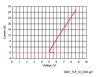
 Figure 6-1 TLP I-V Curve, I/O Pin to GND (tp = 100 ns)
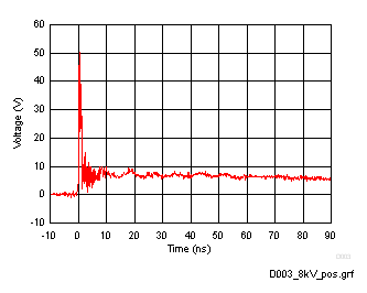
 Figure 6-3 8-kV IEC 61000-4-2 Clamping Voltage Waveform, I/O Pin to GND
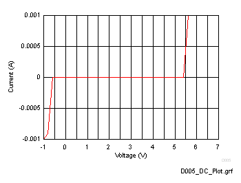
 Figure 6-5 DC Voltage Sweep I-V Curve, I/O Pin to GND
 Figure 6-7 Capacitance vs. Bias Voltage For Different Temperatures (°C)
 Figure 6-9 Insertion Loss vs. Frequency
 Figure 6-2 TLP I-V Curve, GND to I/O Pin (tp = 100 ns)
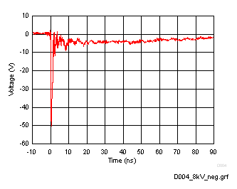
 Figure 6-4 8-kV IEC 61000-4-2 Clamping Voltage Waveform, GND to I/O Pin
 Figure 6-6 Surge Curve (IEC 61000-4-5, tp=8/20 µs), I/O Pin to GND
 Figure 6-8 Leakage Current (at 3.6 V Bias) Across Temperature, I/O Pin to GND