SLVSEN8B July   2018  – October 2023 ESD321

PRODUCTION DATA  

  1.   1
  2. Features
  3. Applications
  4. Description
  5. Revision History
  6. Pin Configuration and Functions
  7. Specifications
    1. 6.1 Absolute Maximum Ratings
    2. 6.2 ESD Ratings – JEDEC Specifications
    3. 6.3 ESD Ratings – IEC Specifications
    4. 6.4 Recommended Operating Conditions
    5. 6.5 Thermal Information
    6. 6.6 Electrical Characteristics
    7. 6.7 Typical Characteristics
  8. Detailed Description
    1. 7.1 Overview
    2. 7.2 Functional Block Diagram
    3. 7.3 Feature Description
    4. 7.4 Device Functional Modes
  9. Application and Implementation
    1. 8.1 Application Information
    2. 8.2 Typical Application
      1. 8.2.1 Design Requirements
      2. 8.2.2 Detailed Design Procedure
        1. 8.2.2.1 Signal Range
        2. 8.2.2.2 Operating Frequency
      3. 8.2.3 Application Curve
    3. 8.3 Power Supply Recommendations
    4. 8.4 Layout
      1. 8.4.1 Layout Guidelines
      2. 8.4.2 Layout Example
  10. Device and Documentation Support
    1. 9.1 Documentation Support
      1. 9.1.1 Related Documentation
    2. 9.2 Receiving Notification of Documentation Updates
    3. 9.3 Support Resources
    4. 9.4 Trademarks
    5. 9.5 Electrostatic Discharge Caution
    6. 9.6 Glossary
  11. 10Mechanical, Packaging, and Orderable Information

Package Options

Mechanical Data (Package|Pins)
Thermal pad, mechanical data (Package|Pins)
Orderable Information

Pin Configuration and Functions

GUID-3384A4AB-ECF4-4559-8BCA-93AB7B05D1C9-low.gifFigure 5-1 DPY Package, 2-Pin X1SON (Top View)
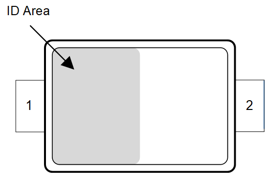
GUID-20210611-CA0I-RDR8-R3QW-0BSB4448BXK6-low.png Figure 5-2 DYA Package, 2-Pin SOD-523 (Top View)
Table 5-1 Pin Functions
PIN TYPE(1) DESCRIPTION
NAME NO.
DPY DYA
IO 1 2 I/O ESD Protected Channel. Connect to the line being protected.
GND 2 1 GND Connect to ground
I = input, O = output, GND = ground