SLVSEG9C May 2018 – February 2024 ESDS311 , ESDS312 , ESDS314
PRODUCTION DATA
- 1
- 1 Features
- 2 Applications
- 3 Description
- 4 Pin Configuration and Functions
- 5 Specifications
- 6 Detailed Description
- 7 Application and Implementation
- 8 Device and Documentation Support
- 9 Revision History
- 10Mechanical, Packaging, and Orderable Information
Package Options
Refer to the PDF data sheet for device specific package drawings
Mechanical Data (Package|Pins)
- DBV|5
Thermal pad, mechanical data (Package|Pins)
Orderable Information
5.7 Typical Characteristics
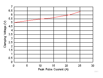 Figure 5-1 Clamping Voltage vs. Peak Pulse Current (tp= 8/20µs), Any IO Pin to GND
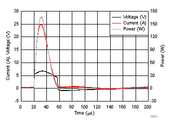 Figure 5-3 Surge Current, Clamping Voltage and Power Curve (tp = 8/20µs), Any IO Pin to GND
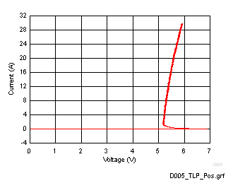 Figure 5-5 TLP I-V Curve, IO to GND, tp = 100ns
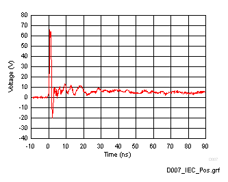 Figure 5-7 +8kV IEC 61000-4-2 Clamping Voltage Waveform
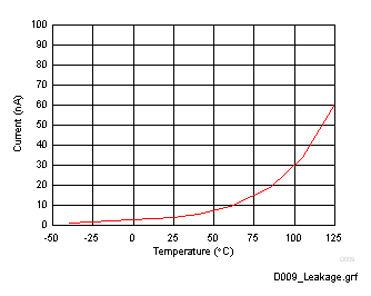 Figure 5-9 DC Leakage vs. Ambient Temperature, Bias Voltage = 3.6V
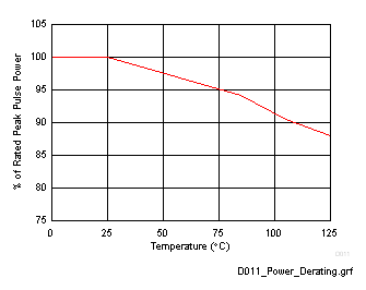 Figure 5-11 Surge Power Derating with Respect To Ambient Temperature
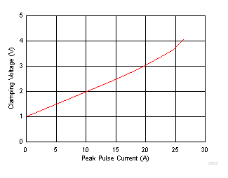 Figure 5-2 Clamping Voltage vs. Peak Pulse Current (tp= 8/20µs), GND to Any IO Pin
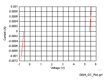 Figure 5-4 DC I-V Curve
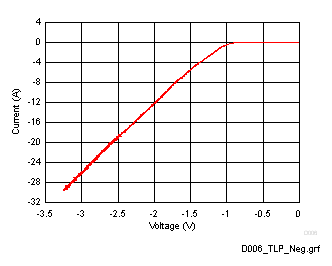 Figure 5-6 TLP I-V Curve, IO to GND Negative, tp=100ns
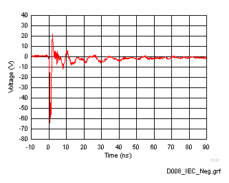 Figure 5-8 -8kV IEC 61000-4-2 Clamping Voltage Waveform
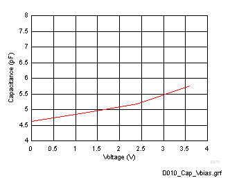 Figure 5-10 Capacitance vs. Bias Voltage at 25 °C
 Figure 5-12 Differential Insertion Loss