SLVSEG9C May 2018 – February 2024 ESDS311 , ESDS312 , ESDS314
PRODUCTION DATA
- 1
- 1 Features
- 2 Applications
- 3 Description
- 4 Pin Configuration and Functions
- 5 Specifications
- 6 Detailed Description
- 7 Application and Implementation
- 8 Device and Documentation Support
- 9 Revision History
- 10Mechanical, Packaging, and Orderable Information
Package Options
Refer to the PDF data sheet for device specific package drawings
Mechanical Data (Package|Pins)
- DBV|5
Thermal pad, mechanical data (Package|Pins)
Orderable Information
4 Pin Configuration and Functions
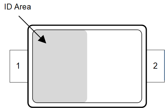
 Figure 4-1 ESDS311 DYF, 2-Pin SOD323 (Top
View)
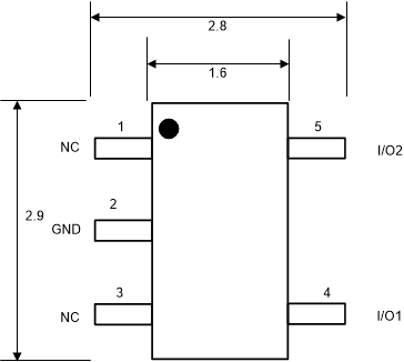
 Figure 4-2 ESDS312 DBV Package, 5-Pin
SOT23 (Top View)
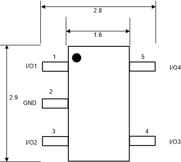
 Figure 4-3 ESDS314 DBV Package, 5-Pin
SOT23 (Top View)
Figure 4-3 ESDS314 DBV Package, 5-Pin
SOT23 (Top View)Table 4-1 Pin Functions for
ESDS311
| PIN | TYPE(1) | DESCRIPTION | |
|---|---|---|---|
| NAME | NO. | ||
| I/O | 1 | I/O | Surge/ESD protected channels. Connect to the lines being protected. |
| GND | 2 | GND | Ground. Connect to ground. |
Table 4-2 Pin Functions for
ESDS312
| PIN | TYPE(1) | DESCRIPTION | |
|---|---|---|---|
| NAME | NO. | ||
| I/O1 | 4 | I/O | Surge/ESD protected channels. Connect to the lines being protected. |
| I/O2 | 5 | ||
| GND | 2 | GND | Ground. Connect to ground. |
| NC | 1 | NC | Not connected; Used for optional straight-through routing. Can be left floating or grounded |
| NC | 3 | ||
Table 4-3 Pin Functions for
ESDS314
| PIN | TYPE(1) | DESCRIPTION | |
|---|---|---|---|
| NAME | NO. | ||
| I/O1 | 1 | I/O | Surge/ESD protected channels. Connect to the lines being protected. |
| I/O2 | 3 | ||
| I/O3 | 4 | ||
| I/O4 | 5 | ||
| GND | 2 | GND | Ground. Connect to ground |
(1) I = input, O = output, NC = no connection, and GND = ground