SNOSCZ4A April   2015  – October 2024 FDC1004-Q1

PRODUCTION DATA  

  1.   1
  2. Features
  3. Applications
  4. Description
  5. Pin Configuration and Functions
  6. Specifications
    1. 5.1 Absolute Maximum Ratings
    2. 5.2 ESD Ratings
    3. 5.3 Recommended Operating Conditions
    4. 5.4 Thermal Information
    5. 5.5 Electrical Characteristics
    6. 5.6 I2C Interface Voltage Level
    7. 5.7 I2C Interface Timing
    8. 5.8 Typical Characteristics
  7. Detailed Description
    1. 6.1 Overview
    2. 6.2 Functional Block Diagram
    3. 6.3 Feature Description
      1. 6.3.1 The Shield
      2. 6.3.2 The CAPDAC
      3. 6.3.3 Capacitive System Offset Calibration
      4. 6.3.4 Capacitive Gain Calibration
    4. 6.4 Device Functional Modes
      1. 6.4.1 Single Ended Measurement
      2. 6.4.2 Differential Measurement
    5. 6.5 Programming
      1. 6.5.1 Serial Bus Address
      2. 6.5.2 Read/Write Operations
      3. 6.5.3 Device Usage
        1. 6.5.3.1 Measurement Configuration
        2. 6.5.3.2 Triggering Measurements
        3. 6.5.3.3 Wait for Measurement Completion
        4. 6.5.3.4 Read of Measurement Result
    6. 6.6 Register Maps
      1. 6.6.1 Registers
        1. 6.6.1.1 Capacitive Measurement Registers
      2. 6.6.2 Measurement Registers
      3. 6.6.3 Measurement Configuration Registers
      4. 6.6.4 FDC Configuration Register
      5. 6.6.5 Offset Calibration Registers
      6. 6.6.6 Gain Calibration Registers
      7. 6.6.7 Manufacturer ID Register
      8. 6.6.8 Device ID Register
  8. Applications and Implementation
    1. 7.1 Application Information
      1. 7.1.1 Liquid Level Sensor
    2. 7.2 Typical Application
      1. 7.2.1 Design Requirements
      2. 7.2.2 Detailed Design Procedure
      3. 7.2.3 Application Curve
    3. 7.3 Best Design Practices
    4. 7.4 Initialization Set Up
    5. 7.5 Power Supply Recommendations
    6. 7.6 Layout
      1. 7.6.1 Layout Guidelines
      2. 7.6.2 Layout Example
  9. Device and Documentation Support
    1. 8.1 Documentation Support
      1. 8.1.1 Related Documentation
    2. 8.2 Receiving Notification of Documentation Updates
    3. 8.3 Support Resources
    4. 8.4 Trademarks
    5. 8.5 Electrostatic Discharge Caution
    6. 8.6 Glossary
  10. Revision History
  11. 10Mechanical, Packaging, and Orderable Information

Package Options

Mechanical Data (Package|Pins)
Thermal pad, mechanical data (Package|Pins)
Orderable Information

Description

Capacitive sensing with grounded capacitor sensors is a very low-power, low-cost, high-resolution contact-less sensing technique that can be applied to a variety of applications ranging from proximity sensing and gesture recognition to material analysis and remote liquid level sensing. The sensor in a capacitive sensing system is any metal or conductor, allowing for low cost and highly flexible system design.

The FDC1004-Q1 is a high-resolution, AEC-Q100 qualified, 4-channel capacitance-to-digital converter for implementing capacitive sensing solutions. Each channel has a full scale range of ±15pF and can handle a sensor offset capacitance of up to 100pF, which can be either programmed internally or can be an external capacitor for tracking environmental changes over time and temperature. The large offset capacitance capability allows for the use of remote sensors.

The FDC1004-Q1 also includes shield drivers for sensor shields, which can reduce EMI interference and help focus the sensing direction of a capacitive sensor. The small footprint of the FDC1004-Q1 allows for use in space-constrained applications. The FDC1004-Q1 is available in a 10-pin VSSOP package, which allows for optical inspection in production, and features an I2C interface for interfacing to an MCU.
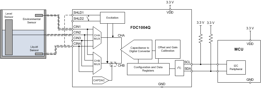
Package Information
PART NUMBER PACKAGE(1) PACKAGE SIZE(2)
FDC1004-Q1 DGS (VSSOP, 10) 3mm × 4.9mm
For all available packages, see Section 10
The package size (length × width) is a nominal value and includes pins, where applicable.
FDC1004-Q1 Typical Application Typical Application