SNOSCZ4A April   2015  – October 2024 FDC1004-Q1

PRODUCTION DATA  

  1.   1
  2. Features
  3. Applications
  4. Description
  5. Pin Configuration and Functions
  6. Specifications
    1. 5.1 Absolute Maximum Ratings
    2. 5.2 ESD Ratings
    3. 5.3 Recommended Operating Conditions
    4. 5.4 Thermal Information
    5. 5.5 Electrical Characteristics
    6. 5.6 I2C Interface Voltage Level
    7. 5.7 I2C Interface Timing
    8. 5.8 Typical Characteristics
  7. Detailed Description
    1. 6.1 Overview
    2. 6.2 Functional Block Diagram
    3. 6.3 Feature Description
      1. 6.3.1 The Shield
      2. 6.3.2 The CAPDAC
      3. 6.3.3 Capacitive System Offset Calibration
      4. 6.3.4 Capacitive Gain Calibration
    4. 6.4 Device Functional Modes
      1. 6.4.1 Single Ended Measurement
      2. 6.4.2 Differential Measurement
    5. 6.5 Programming
      1. 6.5.1 Serial Bus Address
      2. 6.5.2 Read/Write Operations
      3. 6.5.3 Device Usage
        1. 6.5.3.1 Measurement Configuration
        2. 6.5.3.2 Triggering Measurements
        3. 6.5.3.3 Wait for Measurement Completion
        4. 6.5.3.4 Read of Measurement Result
    6. 6.6 Register Maps
      1. 6.6.1 Registers
        1. 6.6.1.1 Capacitive Measurement Registers
      2. 6.6.2 Measurement Registers
      3. 6.6.3 Measurement Configuration Registers
      4. 6.6.4 FDC Configuration Register
      5. 6.6.5 Offset Calibration Registers
      6. 6.6.6 Gain Calibration Registers
      7. 6.6.7 Manufacturer ID Register
      8. 6.6.8 Device ID Register
  8. Applications and Implementation
    1. 7.1 Application Information
      1. 7.1.1 Liquid Level Sensor
    2. 7.2 Typical Application
      1. 7.2.1 Design Requirements
      2. 7.2.2 Detailed Design Procedure
      3. 7.2.3 Application Curve
    3. 7.3 Best Design Practices
    4. 7.4 Initialization Set Up
    5. 7.5 Power Supply Recommendations
    6. 7.6 Layout
      1. 7.6.1 Layout Guidelines
      2. 7.6.2 Layout Example
  9. Device and Documentation Support
    1. 8.1 Documentation Support
      1. 8.1.1 Related Documentation
    2. 8.2 Receiving Notification of Documentation Updates
    3. 8.3 Support Resources
    4. 8.4 Trademarks
    5. 8.5 Electrostatic Discharge Caution
    6. 8.6 Glossary
  10. Revision History
  11. 10Mechanical, Packaging, and Orderable Information

Package Options

Mechanical Data (Package|Pins)
Thermal pad, mechanical data (Package|Pins)
Orderable Information

Single Ended Measurement

The FDC1004-Q1 can be used for interfacing to a single-ended capacitive sensor. In this configuration, connect the sensor to the input CINn (n = 1..4) pins of the FDC1004-Q1 and GND. The capacitance-to-digital convertor (without using the CAPDAC, CAPDAC= 0pF) measures the positive (or the negative) input capacitance in the range of 0pF to 15pF. The CAPDAC can be used for programmable shifting of the input range. In this case it is possible to measure input capacitance in the range of 0pF to ±15pF which are on top of an offset capacitance up to 100pF. In single ended measurements with CAPDAC disabled SHLD1 is internally shorted to SHLD2 (see Figure 6-1); if CAPDAC is enabled SHLD2 is floating (see Figure 6-2). The single ended mode is enabled when the CHB register of the Measurements configuration registers (see Table 6-4) are set to b100 or b111.

FDC1004-Q1 Single-Ended Configuration with CAPDAC DisabledFigure 6-1 Single-Ended Configuration with CAPDAC Disabled
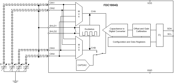
FDC1004-Q1 Single-Ended Configuration with CAPDAC EnabledFigure 6-2 Single-Ended Configuration with CAPDAC Enabled