SNOSCZ5B June 2015 – October 2024 FDC2112 , FDC2114 , FDC2212 , FDC2214
PRODUCTION DATA
- 1
- 1 Features
- 2 Applications
- 3 Description
- 4 Device Comparison
- 5 Pin Configuration and Functions
- 6 Specifications
-
7 Detailed Description
- 7.1 Overview
- 7.2 Functional Block Diagrams
- 7.3 Feature Description
- 7.4 Device Functional Modes
- 7.5 Programming
- 7.6
Register Maps
- 7.6.1 Register List
- 7.6.2 Address 0x00, DATA_CH0
- 7.6.3 Address 0x01, DATA_LSB_CH0 (FDC2212 / FDC2214 only)
- 7.6.4 Address 0x02, DATA_CH1
- 7.6.5 Address 0x03, DATA_LSB_CH1 (FDC2212 / FDC2214 only)
- 7.6.6 Address 0x04, DATA_CH2 (FDC2114, FDC2214 only)
- 7.6.7 Address 0x05, DATA_LSB_CH2 (FDC2214 only)
- 7.6.8 Address 0x06, DATA_CH3 (FDC2114, FDC2214 only)
- 7.6.9 Address 0x07, DATA_LSB_CH3 (FDC2214 only)
- 7.6.10 Address 0x08, RCOUNT_CH0
- 7.6.11 Address 0x09, RCOUNT_CH1
- 7.6.12 Address 0x0A, RCOUNT_CH2 (FDC2114, FDC2214 only)
- 7.6.13 Address 0x0B, RCOUNT_CH3 (FDC2114, FDC2214 only)
- 7.6.14 Address 0x0C, OFFSET_CH0 (FDC21112 / FDC2114 only)
- 7.6.15 Address 0x0D, OFFSET_CH1 (FDC21112 / FDC2114 only)
- 7.6.16 Address 0x0E, OFFSET_CH2 (FDC2114 only)
- 7.6.17 Address 0x0F, OFFSET_CH3 (FDC2114 only)
- 7.6.18 Address 0x10, SETTLECOUNT_CH0
- 7.6.19 Address 0x11, SETTLECOUNT_CH1
- 7.6.20 Address 0x12, SETTLECOUNT_CH2 (FDC2114, FDC2214 only)
- 7.6.21 Address 0x13, SETTLECOUNT_CH3 (FDC2114, FDC2214 only)
- 7.6.22 Address 0x14, CLOCK_DIVIDERS_CH0
- 7.6.23 Address 0x15, CLOCK_DIVIDERS_CH1
- 7.6.24 Address 0x16, CLOCK_DIVIDERS_CH2 (FDC2114, FDC2214 only)
- 7.6.25 Address 0x17, CLOCK_DIVIDERS_CH3 (FDC2114, FDC2214 only)
- 7.6.26 Address 0x18, STATUS
- 7.6.27 Address 0x19, ERROR_CONFIG
- 7.6.28 Address 0x1A, CONFIG
- 7.6.29 Address 0x1B, MUX_CONFIG
- 7.6.30 Address 0x1C, RESET_DEV
- 7.6.31 Address 0x1E, DRIVE_CURRENT_CH0
- 7.6.32 Address 0x1F, DRIVE_CURRENT_CH1
- 7.6.33 Address 0x20, DRIVE_CURRENT_CH2 (FDC2114 / FDC2214 only)
- 7.6.34 Address 0x21, DRIVE_CURRENT_CH3 (FDC2114 / FDC2214 only)
- 7.6.35 Address 0x7E, MANUFACTURER_ID
- 7.6.36 Address 0x7F, DEVICE_ID
- 8 Application and Implementation
- 9 Device and Documentation Support
- 10Revision History
- 11Mechanical, Packaging, and Orderable Information
Package Options
Mechanical Data (Package|Pins)
- DNT|12
Thermal pad, mechanical data (Package|Pins)
Orderable Information
3 Description
Capacitive sensing is a low-power, high-resolution contactless sensing technique that can be applied to a variety of applications ranging from proximity detection and gesture recognition to remote liquid level sensing. The sensor in a capacitive sensing system is any metal or conductor, allowing for a highly flexible system design.
The main challenge limiting sensitivity in capacitive sensing applications is noise susceptibility of the sensors. With the FDC2x1x resonant sensing architecture, performance can be maintained even in the presence of fluorescent light.
The FDC2x1x is a multi-channel family of high-resolution, high-speed capacitance-to-digital converters for implementing capacitive sensing solutions. The devices employ an innovative narrow-band based architecture to offer high rejection of out of band noise while providing high resolution at high speed. The devices support a wide excitation frequency range, offering flexibility in system design. A wide frequency range is especially useful for reliable sensing of conductive liquids such as detergent, soap, and ink.
The FDC221x is optimized for high resolution, up to 28 bits, while the FDC211x offers a fast sample rate of up to 13.3kSPS for easy implementation of applications that use fast moving targets. The large maximum input capacitance of 250nF allows for the use of remote sensors, as well as for tracking environmental changes over time such as temperature and humidity.
The FDC2x1x family targets proximity sensing and liquid level sensing applications for any type of liquids. For non-conductive liquid level sensing applications in the presence of interferences such as human hands, the FDC1004 is recommended and features integrated active shield drivers.
| PART NUMBER | PACKAGE(1) | PACKAGE SIZE(2) |
|---|---|---|
| FDC2112 FDC2212 |
DNT (WSON, 12) | 4mm × 4mm |
| FDC2114 FDC2214 |
RGH (WQFN, 16) | 4mm × 4mm |
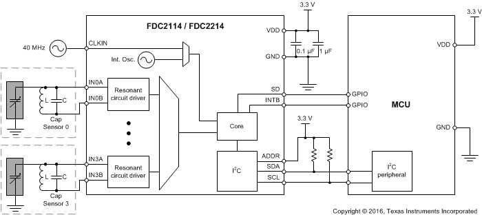
 Simplified Schematic