SNOSCZ5B June 2015 – October 2024 FDC2112 , FDC2114 , FDC2212 , FDC2214
PRODUCTION DATA
- 1
- 1 Features
- 2 Applications
- 3 Description
- 4 Device Comparison
- 5 Pin Configuration and Functions
- 6 Specifications
-
7 Detailed Description
- 7.1 Overview
- 7.2 Functional Block Diagrams
- 7.3 Feature Description
- 7.4 Device Functional Modes
- 7.5 Programming
- 7.6
Register Maps
- 7.6.1 Register List
- 7.6.2 Address 0x00, DATA_CH0
- 7.6.3 Address 0x01, DATA_LSB_CH0 (FDC2212 / FDC2214 only)
- 7.6.4 Address 0x02, DATA_CH1
- 7.6.5 Address 0x03, DATA_LSB_CH1 (FDC2212 / FDC2214 only)
- 7.6.6 Address 0x04, DATA_CH2 (FDC2114, FDC2214 only)
- 7.6.7 Address 0x05, DATA_LSB_CH2 (FDC2214 only)
- 7.6.8 Address 0x06, DATA_CH3 (FDC2114, FDC2214 only)
- 7.6.9 Address 0x07, DATA_LSB_CH3 (FDC2214 only)
- 7.6.10 Address 0x08, RCOUNT_CH0
- 7.6.11 Address 0x09, RCOUNT_CH1
- 7.6.12 Address 0x0A, RCOUNT_CH2 (FDC2114, FDC2214 only)
- 7.6.13 Address 0x0B, RCOUNT_CH3 (FDC2114, FDC2214 only)
- 7.6.14 Address 0x0C, OFFSET_CH0 (FDC21112 / FDC2114 only)
- 7.6.15 Address 0x0D, OFFSET_CH1 (FDC21112 / FDC2114 only)
- 7.6.16 Address 0x0E, OFFSET_CH2 (FDC2114 only)
- 7.6.17 Address 0x0F, OFFSET_CH3 (FDC2114 only)
- 7.6.18 Address 0x10, SETTLECOUNT_CH0
- 7.6.19 Address 0x11, SETTLECOUNT_CH1
- 7.6.20 Address 0x12, SETTLECOUNT_CH2 (FDC2114, FDC2214 only)
- 7.6.21 Address 0x13, SETTLECOUNT_CH3 (FDC2114, FDC2214 only)
- 7.6.22 Address 0x14, CLOCK_DIVIDERS_CH0
- 7.6.23 Address 0x15, CLOCK_DIVIDERS_CH1
- 7.6.24 Address 0x16, CLOCK_DIVIDERS_CH2 (FDC2114, FDC2214 only)
- 7.6.25 Address 0x17, CLOCK_DIVIDERS_CH3 (FDC2114, FDC2214 only)
- 7.6.26 Address 0x18, STATUS
- 7.6.27 Address 0x19, ERROR_CONFIG
- 7.6.28 Address 0x1A, CONFIG
- 7.6.29 Address 0x1B, MUX_CONFIG
- 7.6.30 Address 0x1C, RESET_DEV
- 7.6.31 Address 0x1E, DRIVE_CURRENT_CH0
- 7.6.32 Address 0x1F, DRIVE_CURRENT_CH1
- 7.6.33 Address 0x20, DRIVE_CURRENT_CH2 (FDC2114 / FDC2214 only)
- 7.6.34 Address 0x21, DRIVE_CURRENT_CH3 (FDC2114 / FDC2214 only)
- 7.6.35 Address 0x7E, MANUFACTURER_ID
- 7.6.36 Address 0x7F, DEVICE_ID
- 8 Application and Implementation
- 9 Device and Documentation Support
- 10Revision History
- 11Mechanical, Packaging, and Orderable Information
Package Options
Mechanical Data (Package|Pins)
- DNT|12
Thermal pad, mechanical data (Package|Pins)
Orderable Information
7.3.1 Clocking Architecture
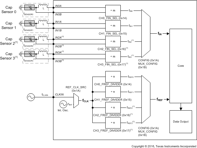
Figure 7-3 shows the clock dividers and multiplexers of the FDC.

In Figure 7-3, the key clocks are fIN, fREF, and fCLK. fCLK is selected from either the internal clock source or external clock source (CLKIN) . The frequency measurement reference clock, fREF, is derived from the fCLK source. TI recommends that precision applications use an external controller clock that offers the stability and accuracy requirements needed for the application. The internal oscillator can be used in applications that require low cost and do not require high precision. The fINx clock is derived from sensor frequency for a channel x, fSENSORx. fREFx and fINx must meet the requirements listed in Table 7-1, depending on whether fCLK (controller clock) is the internal or external clock.
| MODE(1) | CLKIN SOURCE | VALID fREFx RANGE (MHz) | VALID fINx RANGE | SET CHx_FIN_SEL to (2) | SET CHx_SETTLECOUNT to | SET CHx_RCOUNT to |
|---|---|---|---|---|---|---|
| Multi-channel | Internal | fREFx ≤ 55 | < fREFx /4 | Differential sensor configuration: b01: 0.01MHz to 8.75MHz (divide by 1) b10: 5MHz to 10MHz (divide by 2) Single-ended sensor configuration b10: 0.01MHz to 10MHz (divide by 2) | > 3 | > 8 |
| External | fREFx ≤ 40 | |||||
| Single-channel | Either external or internal | fREFx ≤ 35 |
Table 7-2 shows the clock configuration registers for all channels.
| CHANNEL(1) | CLOCK | REGISTER | FIELD [ BIT(S) ] | VALUE |
|---|---|---|---|---|
| All | fCLK = Controller Clock Source | CONFIG, addr 0x1A | REF_CLK_SRC [9] | b0 = internal oscillator is used as the controller clock b1 = external clock source is used as the controller clock |
| 0 | fREF0 | CLOCK_DIVIDERS_CH0, addr 0x14 | CH0_FREF_DIVIDER [9:0] | fREF0 = fCLK / CH0_FREF_DIVIDER |
| 1 | fREF1 | CLOCK_DIVIDERS_CH1, addr 0x15 | CH1_FREF_DIVIDER [9:0] | fREF1 = fCLK / CH1_FREF_DIVIDER |
| 2 | fREF2 | CLOCK_DIVIDERS_CH2, addr 0x16 | CH2_FREF_DIVIDER [9:0] | fREF2 = fCLK / CH2_FREF_DIVIDER |
| 3 | fREF3 | CLOCK_DIVIDERS_CH3, addr 0x17 | CH3_FREF_DIVIDER [9:0] | fREF3 = fCLK / CH3_FREF_DIVIDER |
| 0 | fIN0 | CLOCK_DIVIDERS_CH0, addr 0x14 | CH0_FIN_SEL [13:12] | fIN0 = fSENSOR0 / CH0_FIN_SEL |
| 1 | fIN1 | CLOCK_DIVIDERS_CH1, addr 0x15 | CH1_FIN_SEL [13:12] | fIN1 = fSENSOR1 / CH1_FIN_SEL |
| 2 | fIN2 | CLOCK_DIVIDERS_CH2, addr 0x16 | CH2_FIN_SEL [13:12] | fIN2 = fSENSOR2 / CH2_FIN_SEL |
| 3 | fIN3 | CLOCK_DIVIDERS_CH3, addr 0x17 | CH3_FIN_SEL [13:12] | fIN3 = fSENSOR3 / CH3_FIN_SEL |