SLAS907C December   2015  – December 2020 HD3SS214

PRODUCTION DATA  

  1. Features
  2. Applications
  3. Description
  4. Revision History
  5. Pin Configuration and Functions
  6. Specifications
    1. 6.1 Absolute Maximum Ratings (1) (1)
    2. 6.2 ESD Ratings
    3. 6.3 Recommended Operating Conditions
    4. 6.4 Thermal Information
    5. 6.5 Electrical Characteristics
    6. 6.6 Electrical Characteristics, Device Parameters
    7. 6.7 Timing Requirements
    8. 6.8 Typical Characteristics
  7. Detailed Description
    1. 7.1 Overview
    2. 7.2 Functional Block Diagram
    3. 7.3 Feature Description
      1. 7.3.1 High Speed Switching
      2. 7.3.2 HPD, AUX, and DDC Switching
      3. 7.3.3 Output Enable and Power Savings
    4. 7.4 Device Functional Modes
  8. Application and Implementation
    1. 8.1 Application Information
    2. 8.2 Typical Application
      1. 8.2.1 Dual GPU With Docking Station Support
      2. 8.2.2 Design Requirements
      3. 8.2.3 Detailed Design Procedure
        1. 8.2.3.1 DP Inputs
        2. 8.2.3.2 Source Selection Interface
      4. 8.2.4 DP++ Support
        1. 8.2.4.1 Design Requirements
        2. 8.2.4.2 Detailed Design Procedure
          1. 8.2.4.2.1 AUX and DDC Switching
          2. 8.2.4.2.2 CONFIG1 and CONFIG2 Routing
  9. Power Supply Recommendations
  10. 10Layout
    1. 10.1 Layout Guidelines
      1. 10.1.1 Layer Stack
      2. 10.1.2 Differential Traces
    2. 10.2 Layout Example
  11. 11Device and Documentation Support
    1. 11.1 Device Support
    2. 11.2 Receiving Notification of Documentation Updates
    3. 11.3 Community Resources
    4. 11.4 Trademarks
  12. 12Mechanical, Packaging, and Orderable Information

Package Options

Mechanical Data (Package|Pins)
Thermal pad, mechanical data (Package|Pins)
Orderable Information
CONFIG1 and CONFIG2 Routing

The HD3SS214 only routes the high speed main link, AUX, and Hot Plug Detect (HPD) lines, which means CONFIG1 and CONFIG2 lines need to be routed externally. This is necessary because these lines are important for DP++ as CONFIG1 carries the CAD signal.

A Texas Instruments TS3USB221 (SCDS263) is used to route these signals. It is a 2:1/1:2 USB switch that operates similarly to the HD3SS214. Each port has two inputs, so it is ideal for the CONFIG signals. SRC_SEL is used to select which source the CONFIG signals are from. The circuit for routing these signals can be seen in Figure 8-5.
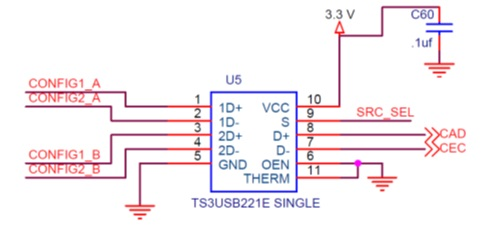
GUID-5F5C4600-50DC-4B36-B718-BD48F9461998-low.pngFigure 8-5 CONFIG Signal Routing