SLAS907C December 2015 – December 2020 HD3SS214
PRODUCTION DATA
- 1 Features
- 2 Applications
- 3 Description
- 4 Revision History
- 5 Pin Configuration and Functions
- 6 Specifications
- 7 Detailed Description
- 8 Application and Implementation
- 9 Power Supply Recommendations
- 10Layout
- 11Device and Documentation Support
- 12Mechanical, Packaging, and Orderable Information
Package Options
Mechanical Data (Package|Pins)
- ZXH|50
Thermal pad, mechanical data (Package|Pins)
Orderable Information
8.2.4.2.1 AUX and DDC Switching
The HD3SS214 supports DP++ implementations.
According to the DP++ standard, the DP AUX line is repurposed as the DDC line when HDMI signals are being transmitted. Unfortunately, the AUX and DDC signals have very different electrical requirements. AUX is a differential signal that requires AC coupling, while DDC uses I2C protocol, which needs pull-up resistors. As a result, these signals are electrically incompatible if extra circuitry is not designed to accommodate the signals.
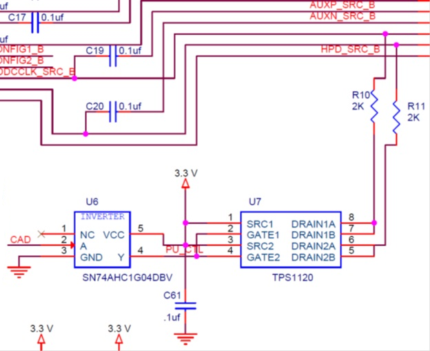
The source selection design block uses conditional pull-up resistors to support AUX and DDC signals on a unified line.Figure 8-4 illustrates the circuit that was used to enable the signal.
 Figure 8-4 Combined AUX/DDC Circuitry
In this circuit, the unified AUX/DDC lines are split into two branches prior to entering the HD3SS214. One branch is AC coupled and is connected to the AUX inputs of the HD3SS214. The other is connected to the DDC inputs. AUX_SEL is configured so that the HD3SS214 transmits both of these through the switch. A conditional pull-up resistor system is connected to the DDC branch of the line. This resistor system will enable the pull-up resistors on the line only when HDMI/DVI signals are being transmitted, that is, when AUX is transmitting DDC signals. This prevents the AUX signal from being interfered with during standard DP mode and enables I2C DDC signaling during HDMI/DVI mode
The control input for the conditional pull-up circuit is the Cable Adaptor Detect (CAD) signal. When an HDMI or DVI sink is being used, this signal goes high, which indicates that the AUX line must transmit the DDC signal. When a standard DP sink is being used, the CAD signal goes low, indicating that the AUX line is transmitting its normal AUX signal. In this way, the CAD signal indicates when the AUX/DDC lines need pull-up resistors and when they do not.
The conditional pull-up circuit consists of an inverter, a p-type MOSFET, and two pull-up resistors. The FET acts as a switch between the pull-up resistors. When CAD is high (indicating that pull-up resistors are needed), the inverter outputs a low signal, which brings the Vgs of the FET below the FET’s threshold voltage. Pulling Vgs below the threshold voltage turns the p-type FET on. When the FET turns on, it connects the AUX line’s pull-up resistors to VCC, which enables them.
The chosen inverter is a Texas Instruments SN74AHC1G04 inverter, which has very fast response times and very good electrical characteristics for VOH and VOL. The MOSFET chosen is a Texas Instruments TPS1120 (SLVS080). This device has a convenient dual transistor package, an ideal threshold voltage and very low drain-to-source resistance when on. Together, these two devices have a desirable noise margin of 0.9 V.