SLLSES1D December 2015 – September 2020 HD3SS3220
PRODUCTION DATA
- 1 Features
- 2 Applications
- 3 Description
- 4 Revision History
- 5 Pin Configuration and Functions
- 6 Specifications
-
7 Detailed Description
- 7.1 Overview
- 7.2 Functional Block Diagram
- 7.3
Feature Description
- 7.3.1 DFP/Source – Downstream Facing Port
- 7.3.2 UFP/Sink – Upstream Facing Port
- 7.3.3 DRP – Dual Role Port
- 7.3.4 Cable Orientation and Mux Control
- 7.3.5 Type-C Current Mode
- 7.3.6 Accessory Support
- 7.3.7 Audio Accessory
- 7.3.8 Debug Accessory
- 7.3.9 VCONN support for Active Cables
- 7.3.10 I2C and GPIO Control
- 7.3.11 HD3SS3220 V(BUS) Detection
- 7.3.12 VDD5 and VCC33 Power-On Requirements
- 7.4 Device Functional Modes
- 7.5 Programming
- 7.6
Register Maps
- 7.6.1 Device Identification Register (offset = 0x07 through 0x00) [reset = 0x00, 0x54, 0x55, 0x53, 0x42, 0x33, 0x32, 0x32]
- 7.6.2 Connection Status Register (offset = 0x08) [reset = 0x00]
- 7.6.3 Connection Status and Control Register (offset = 0x09) [reset = 0x20]
- 7.6.4 General Control Register (offset = 0x0A) [reset = 0x00]
- 7.6.5 Device Revision Register (offset = 0xA0) [reset = 0x02]
- 8 Application and Implementation
-
9 Layout
- 9.1
Layout Guidelines
- 9.1.1 Suggested PCB Stackups
- 9.1.2 High-Speed Signal Trace Length Matching
- 9.1.3 Differential Signal Spacing
- 9.1.4 High-Speed Differential Signal Rules
- 9.1.5 Symmetry in the Differential Pairs
- 9.1.6 Via Discontinuity Mitigation
- 9.1.7 Surface-Mount Device Pad Discontinuity Mitigation
- 9.1.8 ESD/EMI Considerations
- 9.2 Layout
- 9.1
Layout Guidelines
- 10Device and Documentation Support
- 11Mechanical, Packaging, and Orderable Information
Package Options
Mechanical Data (Package|Pins)
- RNH|30
Thermal pad, mechanical data (Package|Pins)
Orderable Information
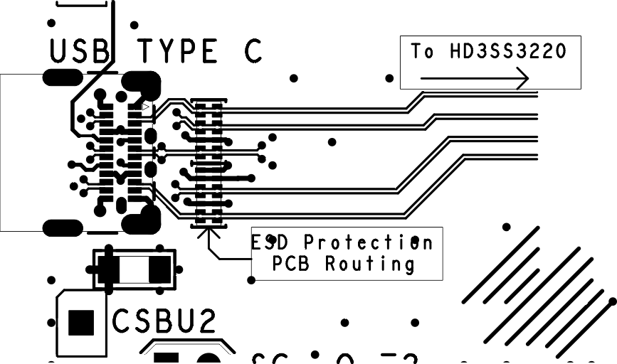
9.2 Layout
 Figure 9-10 Layout Example
 Figure 9-11 Layout Example 2