SLLSES1D December 2015 – September 2020 HD3SS3220
PRODUCTION DATA
- 1 Features
- 2 Applications
- 3 Description
- 4 Revision History
- 5 Pin Configuration and Functions
- 6 Specifications
-
7 Detailed Description
- 7.1 Overview
- 7.2 Functional Block Diagram
- 7.3
Feature Description
- 7.3.1 DFP/Source – Downstream Facing Port
- 7.3.2 UFP/Sink – Upstream Facing Port
- 7.3.3 DRP – Dual Role Port
- 7.3.4 Cable Orientation and Mux Control
- 7.3.5 Type-C Current Mode
- 7.3.6 Accessory Support
- 7.3.7 Audio Accessory
- 7.3.8 Debug Accessory
- 7.3.9 VCONN support for Active Cables
- 7.3.10 I2C and GPIO Control
- 7.3.11 HD3SS3220 V(BUS) Detection
- 7.3.12 VDD5 and VCC33 Power-On Requirements
- 7.4 Device Functional Modes
- 7.5 Programming
- 7.6
Register Maps
- 7.6.1 Device Identification Register (offset = 0x07 through 0x00) [reset = 0x00, 0x54, 0x55, 0x53, 0x42, 0x33, 0x32, 0x32]
- 7.6.2 Connection Status Register (offset = 0x08) [reset = 0x00]
- 7.6.3 Connection Status and Control Register (offset = 0x09) [reset = 0x20]
- 7.6.4 General Control Register (offset = 0x0A) [reset = 0x00]
- 7.6.5 Device Revision Register (offset = 0xA0) [reset = 0x02]
- 8 Application and Implementation
-
9 Layout
- 9.1
Layout Guidelines
- 9.1.1 Suggested PCB Stackups
- 9.1.2 High-Speed Signal Trace Length Matching
- 9.1.3 Differential Signal Spacing
- 9.1.4 High-Speed Differential Signal Rules
- 9.1.5 Symmetry in the Differential Pairs
- 9.1.6 Via Discontinuity Mitigation
- 9.1.7 Surface-Mount Device Pad Discontinuity Mitigation
- 9.1.8 ESD/EMI Considerations
- 9.2 Layout
- 9.1
Layout Guidelines
- 10Device and Documentation Support
- 11Mechanical, Packaging, and Orderable Information
Package Options
Mechanical Data (Package|Pins)
- RNH|30
Thermal pad, mechanical data (Package|Pins)
Orderable Information
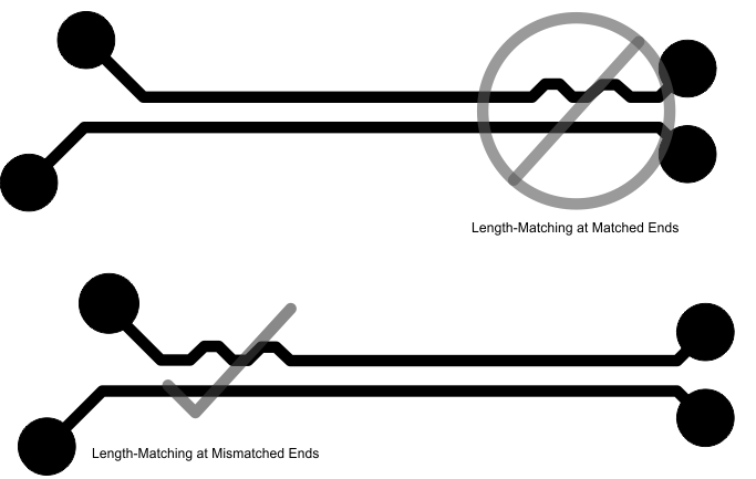
9.1.2 High-Speed Signal Trace Length Matching
Match the etch lengths of the relevant differential pair traces of each interface. The etch length of the differential pair groups do not need to match (that is, the length of the transmit pair does not need to match the length of the receive pair). When matching the intrapair length of the high-speed signals, add serpentine routing to match the lengths as close to the mismatched ends as possible. See Figure 9-1 for more details.
 Figure 9-1 Length Matching