SLLSEM7D January 2015 – January 2017 HD3SS460
PRODUCTION DATA.
- 1 Features
- 2 Applications
- 3 Description
- 4 Revision History
- 5 Device Comparison Table
- 6 Pin Configuration and Functions
- 7 Specifications
- 8 Detailed Description
- 9 Application and Implementation
- 10Power Supply Recommendations
- 11Layout
- 12Device and Documentation Support
- 13Mechanical, Packaging, and Orderable Information
Package Options
Refer to the PDF data sheet for device specific package drawings
Mechanical Data (Package|Pins)
- RNH|30
- RHR|28
Thermal pad, mechanical data (Package|Pins)
- RHR|28
Orderable Information
1 Features
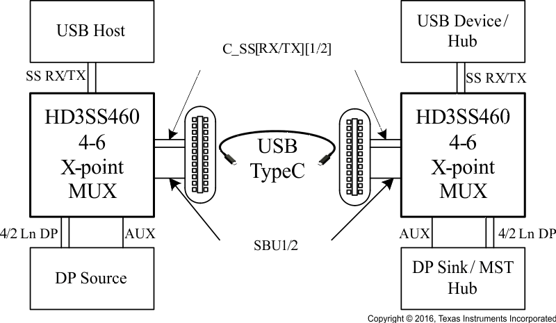
- Provides MUX Solution for USB Type-CTM Ecosystem Including Alternate Mode (AM)
- Provides Wide Channel Selection Choices Including USBSS and 2 Ch AM, 4 Ch AM
- Compatible with 5 Gbps USB3.1 Gen 1 and AM Including 5.4 Gbps DisplayPort 1.2a
- Compatible for Source/Host and Sink/Device Applications
- Provides Cross-point MUX for Low Speed SBU Pins
- Bidirectional "Mux/De-Mux" Differential Switch
- Supports Common Mode Voltage 0-2 V
- Low Power with 1-μA Shutdown and 0.6 mA Active
- Single Supply Voltage VCC of 3.3 V ±10%
- Industrial Temperature Range of –40 to 85°C
2 Applications
- Flippable USB Type-CTM Ecosystem
- Tablets, Laptops, Monitors, Phones
- USB Host and Devices
- Docking Stations
3 Description
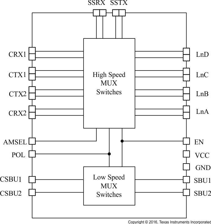
The HD3SS460 is a high-speed bi-directional passive switch in mux or demux configurations. Based on control pin POL the device provides switching to accommodate connector flipping. The device also provides muxing between 2Ch Data / 2Ch Video and all 4Ch Video based on control pin AMSEL.
The device also provides cross points MUX for low speed pins as needed in flippable connector implementation.
The HD3SS460 is a generic analog differential passive switch that can work for any high speed interface applications as long as it is biased at a common mode voltage range of 0-2V and has differential signaling with differential amplitude up to 1800mVpp. It employs an adaptive tracking that ensures the channel remains unchanged for entire common mode voltage range.
Excellent dynamic characteristics of the device allow high speed switching with minimum attenuation to the signal eye diagram with very little added jitter. It consumes <2 mW of power when operational and <5µW in shutdown mode, exercisable by EN pin.
Device Information(1)
| PART NUMBER | PACKAGE | BODY SIZE (NOM) |
|---|---|---|
| HD3SS460 | QFN (RHR) (28) | 3.50 mm × 5.50 mm |
| HD3SS460I | ||
| HD3SS460 | QFN (RNH) (30) | 2.50 mm × 4.50 mm |
| HD3SS460I |
- For all available packages, see the orderable addendum at the end of the data sheet.
sp
Simplified Schematic

Application
