SNAS693D July 2017 – February 2021 HDC2010
PRODUCTION DATA
- 1
- 1 Features
- 2 Applications
- 3 Description
- 4 Revision History
- 5 Pin Configuration and Functions
- 6 Specifications
-
7 Detailed Description
- 7.1 Overview
- 7.2 Functional Block Diagram
- 7.3 Feature Description
- 7.4 Device Functional Modes
- 7.5 Programming
- 7.6
Register Maps
- 7.6.1 Address 0x00 Temperature LSB
- 7.6.2 Address 0x01 Temperature MSB
- 7.6.3 Address 0x02 Humidity LSB
- 7.6.4 Address 0x03 Humidity MSB
- 7.6.5 Address 0x04 Interrupt DRDY
- 7.6.6 Address 0x05 Temperature MAX
- 7.6.7 Address 0x06 Humidity MAX
- 7.6.8 Address 0x07 Interrupt Configuration
- 7.6.9 Address 0x08 Temperature Offset Adjustment
- 7.6.10 47
- 7.6.11 Address 0x09 Humidity Offset Adjustment
- 7.6.12 49
- 7.6.13 Address 0x0A Temperature Threshold LOW
- 7.6.14 Address 0x0B Temperature Threshold HIGH
- 7.6.15 Address 0x0C Humidity Threshold LOW
- 7.6.16 Address 0x0D Humidity Threshold HIGH
- 7.6.17 Address 0x0E Reset and DRDY/INT Configuration Register
- 7.6.18 Address 0x0F Measurement Configuration
- 7.6.19 Manufacturer ID Low
- 7.6.20 Manufacturer ID High
- 7.6.21 Device ID Low
- 7.6.22 Device ID High
- 8 Application and Implementation
- 9 Power Supply Recommendations
- 10Layout
- 11Device and Documentation Support
- 12Mechanical, Packaging, and Orderable Information
Package Options
Refer to the PDF data sheet for device specific package drawings
Mechanical Data (Package|Pins)
- YPA|6
Thermal pad, mechanical data (Package|Pins)
Orderable Information
5 Pin Configuration and Functions
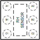
 Figure 5-1 WLCSP
(DSBGA)6-Pin YPATop View
Figure 5-1 WLCSP
(DSBGA)6-Pin YPATop ViewTable 5-1 Pin Functions
| PIN | I/O TYPE(1) | DESCRIPTION | |
|---|---|---|---|
| NAME | NO. | ||
| VDD | A1 | P | Positive Supply Voltage |
| ADDR | B1 | I | Address select pin – hardwired to VDD or GND. GND: slave address: 1000000 VDD: slave address: 1000001 |
| GND | C1 | G | Ground |
| SDA | A2 | I/O | Serial data line for I2C, open-drain; requires a pullup resistor to VDD |
| SCL | B2 | I | Serial clock line for I2C, open-drain; requires a pullup resistor to VDD |
| DRDY / INT | C2 | O | Data ready/Interrupt. Push-pull output |
(1) P=Power, G=Ground, I=Input, O=Output