SBOS069A October   1997  – December 2024 INA122

PRODUCTION DATA  

  1.   1
  2. Features
  3. Applications
  4. Description
  5. Pin Configuration and Functions
  6. Specifications
    1. 5.1 Absolute Maximum Ratings
    2. 5.2 Recommended Operating Conditions
    3. 5.3 Thermal Information
    4. 5.4 Electrical Characteristics
    5. 5.5 Typical Characteristics
  7. Detailed Description
    1. 6.1 Overview
    2. 6.2 Functional Block Diagram
    3. 6.3 Feature Description
      1. 6.3.1 Setting the Gain
      2. 6.3.2 Input Common-Mode Range
      3. 6.3.3 Input Protection
      4. 6.3.4 Output Current Range
    4. 6.4 Device Functional Modes
  8. Application and Implementation
    1. 7.1 Application Information
      1. 7.1.1 Offset Trimming
      2. 7.1.2 Input Bias Current Return Path
    2. 7.2 Typical Application
      1. 7.2.1 Resistive-Bridge Pressure Sensor
        1. 7.2.1.1 Design Requirements
        2. 7.2.1.2 Detailed Design Procedure
        3. 7.2.1.3 Application Curve
    3. 7.3 Power Supply Recommendations
    4. 7.4 Layout
      1. 7.4.1 Layout Guidelines
      2. 7.4.2 Layout Example
  9. Device and Documentation Support
    1. 8.1 Device Support
      1. 8.1.1 Development Support
        1. 8.1.1.1 PSpice® for TI
        2. 8.1.1.2 TINA-TI (Free Software Download)
    2. 8.2 Receiving Notification of Documentation Updates
    3. 8.3 Support Resources
    4. 8.4 Trademarks
    5. 8.5 Electrostatic Discharge Caution
    6. 8.6 Glossary
  10. Revision History
  11. 10Mechanical, Packaging, and Orderable Information

Package Options

Refer to the PDF data sheet for device specific package drawings

Mechanical Data (Package|Pins)
  • D|8
  • P|8
Thermal pad, mechanical data (Package|Pins)
Orderable Information

Input Common-Mode Range

The input common-mode range of the INA122 can operate over a wide range of power supply and VREF configurations. The common-mode range for some common operating conditions is shown in the performance curves in the Typical Characteristics section, and also in Figure 6-3 and Figure 6-4.
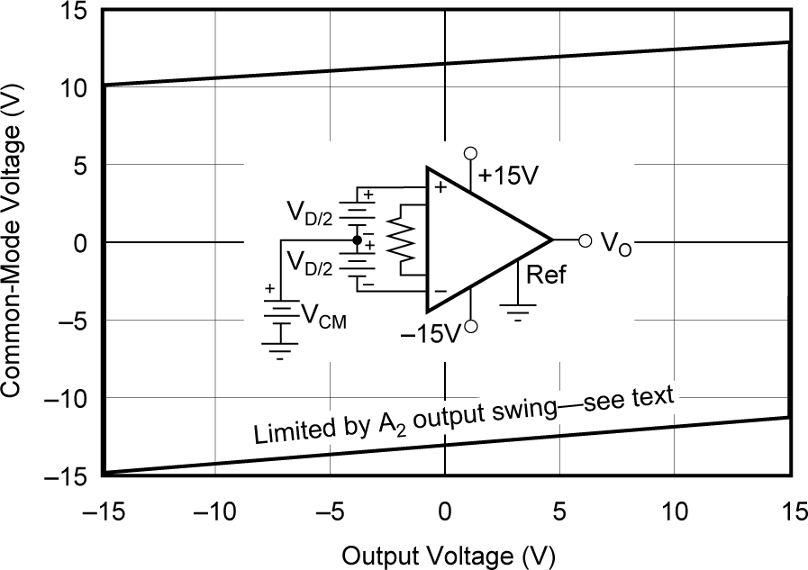
INA122 Input Common-Mode Range vs Output Voltage, Vs = ±15V, G = 5Figure 6-3 Input Common-Mode Range vs Output Voltage, Vs = ±15V, G = 5
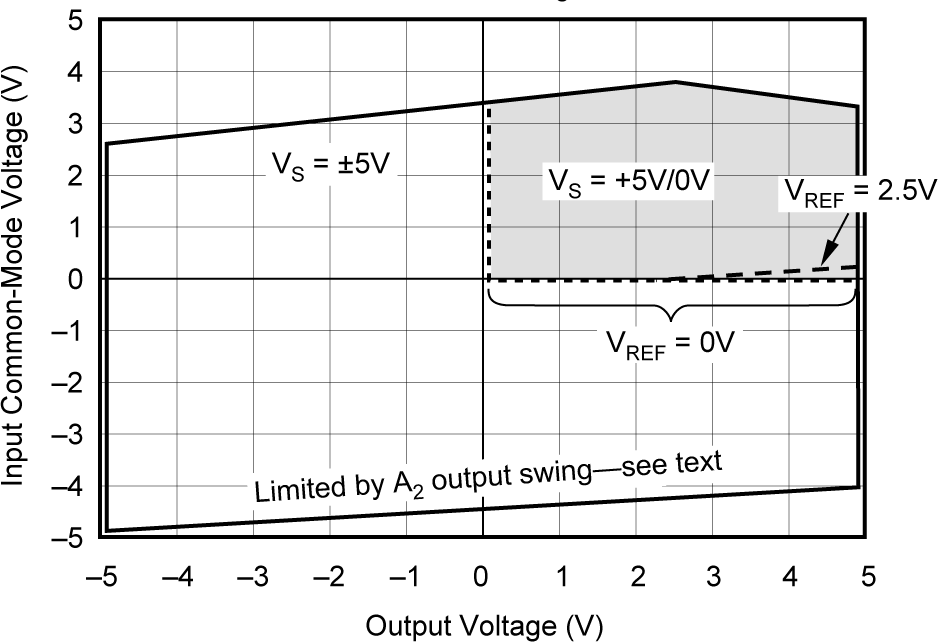
INA122 Input Common-Mode Range vs Output Voltage, Vs = ±5, G = 5Figure 6-4 Input Common-Mode Range vs Output Voltage, Vs = ±5, G = 5