SBOS051F October   1995  – May 2022 INA128 , INA129

PRODUCTION DATA  

  1. Features
  2. Applications
  3. Description
  4. Revision History
  5. Device Comparison Table
  6. Pin Configuration and Functions
  7. Specifications
    1. 7.1 Absolute Maximum Ratings
    2. 7.2 ESD Ratings
    3. 7.3 Recommended Operating Conditions
    4. 7.4 Thermal Information
    5. 7.5 Electrical Characteristics
    6. 7.6 Typical Characteristics
  8. Detailed Description
    1. 8.1 Overview
    2. 8.2 Functional Block Diagram
    3. 8.3 Feature Description
      1. 8.3.1 Noise Performance
    4. 8.4 Device Functional Modes
  9. Application and Implementation
    1. 9.1 Application Information
      1. 9.1.1 Input Common-Mode Range
    2. 9.2 Typical Application
      1. 9.2.1 Design Requirements
      2. 9.2.2 Detailed Design Procedure
        1. 9.2.2.1 Setting the Gain
        2. 9.2.2.2 Dynamic Performance
        3. 9.2.2.3 Offset Trimming
        4. 9.2.2.4 Input Bias Current Return Path
      3. 9.2.3 Application Curves
    3. 9.3 System Examples
  10. 10Power Supply Recommendations
    1. 10.1 Low-Voltage Operation
  11. 11Layout
    1. 11.1 Layout Guidelines
    2. 11.2 Layout Example
  12. 12Device and Documentation Support
    1. 12.1 Device Support
      1. 12.1.1 Development Support
        1. 12.1.1.1 PSpice® for TI
        2. 12.1.1.2 TINA-TI™ Simulation Software (Free Download)
    2. 12.2 Documentation Support
      1. 12.2.1 Related Documentation
    3. 12.3 Receiving Notification of Documentation Updates
    4. 12.4 Support Resources
    5. 12.5 Trademarks
    6. 12.6 Electrostatic Discharge Caution
    7. 12.7 Glossary
  13. 13Mechanical, Packaging, and Orderable Information

Package Options

Mechanical Data (Package|Pins)
Thermal pad, mechanical data (Package|Pins)
Orderable Information

Offset Trimming

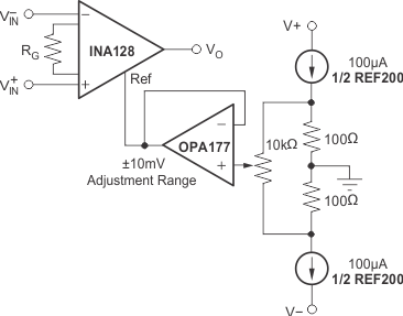
The INA12x is laser trimmed for low-offset voltage and low offset voltage drift. Most applications require no external offset adjustment. Figure 9-2 shows an optional circuit for trimming the output offset voltage. The voltage applied to the REF pin is summed with the output. The op-amp buffer provides low impedance at the REF pin to preserve good common-mode rejection.
GUID-D691C98F-23BE-4FD3-B5C2-4531655CC84B-low.gifFigure 9-2 Optional Trimming of Output Offset Voltage