SGLS174J September   2003  – August 2018 INA138-Q1 , INA168-Q1

PRODUCTION DATA.  

  1. Features
  2. Applications
  3. Description
    1.     Device Images
      1.      Typical Application Circuit
  4. Revision History
  5. Pin Configuration and Functions
    1.     Pin Functions
  6. Specifications
    1. 6.1 Absolute Maximum Ratings
    2. 6.2 ESD Ratings
    3. 6.3 Recommended Operating Conditions
    4. 6.4 Thermal Information
    5. 6.5 Electrical Characteristics
    6. 6.6 Typical Characteristics
  7. Detailed Description
    1. 7.1 Overview
    2. 7.2 Functional Block Diagram
    3. 7.3 Feature Description
      1. 7.3.1 Output Voltage Range
      2. 7.3.2 Bandwidth
    4. 7.4 Device Functional Modes
  8. Application and Implementation
    1. 8.1 Application Information
      1. 8.1.1 Operation
    2. 8.2 Typical Applications
      1. 8.2.1 Buffering Output to Drive an ADC
        1. 8.2.1.1 Design Requirements
        2. 8.2.1.2 Detailed Design Procedure
          1. 8.2.1.2.1 Selecting RS and RL
        3. 8.2.1.3 Application Curve
      2. 8.2.2 Output Filter
        1. 8.2.2.1 Design Requirements
        2. 8.2.2.2 Detailed Design Procedure
        3. 8.2.2.3 Application Curve
      3. 8.2.3 Offsetting the Output Voltage
      4. 8.2.4 Bipolar Current Measurement
        1. 8.2.4.1 Application Curve
      5. 8.2.5 Bipolar Current Measurement Using Differential Input of an ADC
      6. 8.2.6 Multiplexed Measurement Using Logic Signal for Power
  9. Power Supply Recommendations
  10. 10Layout
    1. 10.1 Layout Guidelines
    2. 10.2 Layout Example
  11. 11Device and Documentation Support
    1. 11.1 Documentation Support
      1. 11.1.1 Related Documentation
    2. 11.2 Related Links
    3. 11.3 Receiving Notification of Documentation Updates
    4. 11.4 Community Resources
    5. 11.5 Trademarks
    6. 11.6 Electrostatic Discharge Caution
    7. 11.7 Glossary
  12. 12Mechanical, Packaging, and Orderable Information

Package Options

Mechanical Data (Package|Pins)
Thermal pad, mechanical data (Package|Pins)
Orderable Information

Multiplexed Measurement Using Logic Signal for Power

Measure multiple loads as shown in Figure 18. In this configuration, each INA138-Q1 or INA168-Q1 device is powered by the digital I/O from the ADS7870. Multiplexing is achieved by switching on or off each desired I/O.
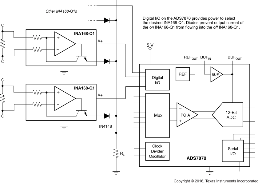
INA138-Q1 INA168-Q1 multiplexmeas_logic_gls174.gifFigure 18. Multiplexed Measurement Using Logic Signal for Power