SBOS052A september 2000 – august 2023 INA141
PRODUCTION DATA
- 1
- 1Features
- 2Applications
- 3Description
- 4Revision History
- 5Pin Configuration and Functions
- 6Specifications
- 7Application and Implementation
- 8Device and Documentation Support
- 9Mechanical, Packaging, and Orderable Information
Package Options
Mechanical Data (Package|Pins)
- D|8
Thermal pad, mechanical data (Package|Pins)
Orderable Information
7.1 Application Information
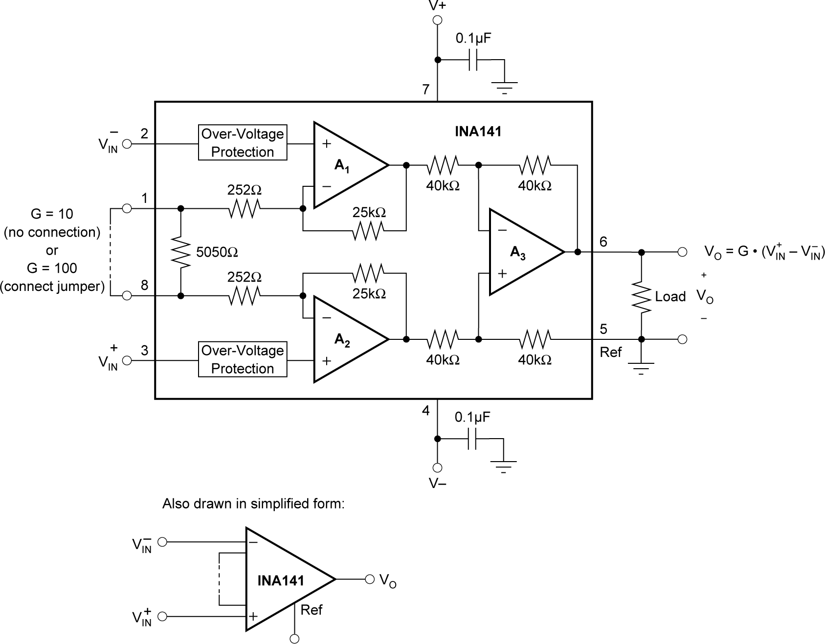
Figure 7-1 shows the basic connections required for operation of the INA141. Applications with noisy or high impedance power supplies can require decoupling capacitors close to the device pins as shown.
 Figure 7-1 Basic Connections.
The output is referred to the output reference (Ref) pin, which is normally grounded. This connection must be low-impedance to maintain good common-mode rejection. A resistance of 8 Ω in series with the Ref pin causes a typical device to degrade to approximately 80 dB CMR (G = 10 V/V).