SBOS109A September 1999 – November 2023 INA146
PRODUCTION DATA
- 1
- 1Features
- 2Applications
- 3Description
- 4Pin Configuration and Functions
- 5Specifications
- 6Application and Implementation
- 7Device and Documentation Support
- 8Revision History
- 9Mechanical, Packaging, and Orderable Information
Package Options
Mechanical Data (Package|Pins)
- D|8
Thermal pad, mechanical data (Package|Pins)
Orderable Information
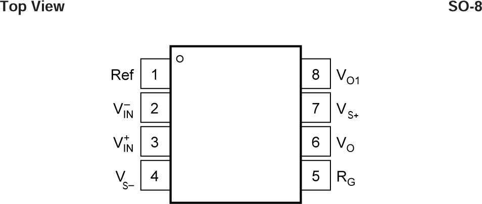
4 Pin Configuration and Functions
 Figure 4-1 INA146 D Package, 8-Pin SOIC (Top
View)
Figure 4-1 INA146 D Package, 8-Pin SOIC (Top
View)Table 4-1 Pin Functions
| PIN | TYPE(1) | DESCRIPTION | |
|---|---|---|---|
| NAME | NO. | ||
| Ref | 1 | I | Reference input. This pin must be driven by a low impedance source. |
| VIN- | 2 | I | Negative (inverting) input |
| VIN+ | 3 | I | Positive (non-inverting) input |
| VS− | 4 | − | Negative supply |
| RG | 5 | I | Gain setting input. Place a resistor network between pin 1 and pin 5. |
| VO | 6 | O | Output of amplifier A2 |
| VS+ | 7 | − | Positive supply |
| VO1 | 8 | O | Output of amplifier A1 |
(1) Signal Types: I = Input, O = Output, I/O
= Input or Output.