SBOS859B March   2018  – July 2018 INA1620

PRODUCTION DATA.  

  1. Features
  2. Applications
  3. Description
    1.     Device Images
      1.      INA1620 Simplified Internal Schematic
      2.      FFT: 1 kHz, 32-Ω Load, 50 mW
  4. Revision History
  5. Pin Configuration and Functions
    1.     Pin Functions
  6. Specifications
    1. 6.1 Absolute Maximum Ratings
    2. 6.2 ESD Ratings
    3. 6.3 Recommended Operating Conditions
    4. 6.4 Thermal Information
    5. 6.5 Electrical Characteristics:
    6. 6.6 Typical Characteristics
  7. Detailed Description
    1. 7.1 Overview
    2. 7.2 Functional Block Diagram
    3. 7.3 Feature Description
      1. 7.3.1 Matched Thin-Film Resistor Pairs
      2. 7.3.2 Power Dissipation
      3. 7.3.3 Thermal Shutdown
      4. 7.3.4 EN Pin
      5. 7.3.5 GND Pin
      6. 7.3.6 Input Protection
    4. 7.4 Device Functional Modes
      1. 7.4.1 Shutdown Mode
      2. 7.4.2 Output Transients During Power Up and Power Down
  8. Application and Implementation
    1. 8.1 Application Information
      1. 8.1.1 Noise Performance
      2. 8.1.2 Resistor Tolerance
      3. 8.1.3 EMI Rejection
      4. 8.1.4 EMIRR +IN Test Configuration
    2. 8.2 Typical Application
      1. 8.2.1 Design Requirements
      2. 8.2.2 Detailed Design Procedure
      3. 8.2.3 Application Curves
    3. 8.3 Other Application Examples
      1. 8.3.1 Preamplifier for Professional Microphones
  9. Power Supply Recommendations
  10. 10Layout
    1. 10.1 Layout Guidelines
    2. 10.2 Layout Example
  11. 11Device and Documentation Support
    1. 11.1 Device Support
      1. 11.1.1 Development Support
        1. 11.1.1.1 TINA-TI (Free Software Download)
        2. 11.1.1.2 TI Precision Designs
    2. 11.2 Documentation Support
      1. 11.2.1 Related Documentation
    3. 11.3 Receiving Notification of Documentation Updates
    4. 11.4 Community Resources
    5. 11.5 Trademarks
    6. 11.6 Electrostatic Discharge Caution
    7. 11.7 Glossary
  12. 12Mechanical, Packaging, and Orderable Information

Package Options

Mechanical Data (Package|Pins)
Thermal pad, mechanical data (Package|Pins)
Orderable Information

EN Pin

The enable pin (EN) of the INA1620 is used to toggle the amplifier enabled and disabled states. The logic levels defining these two states are: VEN ≤ 0.78 V (shutdown mode), and VEN ≥ 0.82 V (enabled). These threshold levels are referenced to the device ground (GND) pin. The EN pin can be driven by a GPIO pin from the system controller, discrete logic gates, or can be connected directly to the V+ supply. Do not leave the EN pin floating because the amplifier is prevented from being enabled. Likewise, do not place GPIO pins used to control the EN pin in a high-impedance state because this placement also prevents the amplifier from being enabled. A small current flows into the enable pin when a voltage is applied. Using the simplified internal schematic shown in Figure 46, use Equation 4 to estimate the enable pin current:

Equation 4. INA1620 ai_enable_eq.gif

As illustrated in Figure 46, the EN pin is protected by diodes to the amplifier power supplies. Do not connect the EN pin to voltages outside the limits defined in the Specifications section.
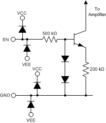
INA1620 d304_enable_u.gifFigure 46. EN Pin Simplified Internal Schematic