SBOS859B March 2018 – July 2018 INA1620
PRODUCTION DATA.
- 1 Features
- 2 Applications
- 3 Description
- 4 Revision History
- 5 Pin Configuration and Functions
- 6 Specifications
- 7 Detailed Description
- 8 Application and Implementation
- 9 Power Supply Recommendations
- 10Layout
- 11Device and Documentation Support
- 12Mechanical, Packaging, and Orderable Information
Package Options
Mechanical Data (Package|Pins)
- RTW|24
Thermal pad, mechanical data (Package|Pins)
- RTW|24
Orderable Information
8.2 Typical Application
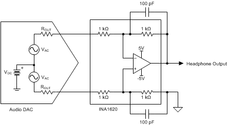
The low distortion and high output-current capabilities of the INA1620 make this device an excellent choice for headphone-amplifier applications in portable or studio applications. These applications typically employ an audio digital-to-analog converter (DAC) and a separate headphone amplifier circuit connected to the DAC output. High-performance audio DACs can have an output signal that is either a varying current or voltage. Voltage output configurations require less external circuitry, and therefore have advantages in cost, power consumption, and solution size. However, these configurations can offer slightly lower performance than current output configurations. Differential outputs are standard on both types of DACs. Differential outputs double the output signal levels that can be delivered on a single, low-voltage supply, and also allow for even-harmonics common to both outputs to be cancelled by external circuitry. A simplified representation of a voltage-output audio DAC is shown in Figure 55. Two ac voltage sources (VAC) deliver the output signal to the complementary outputs through their associated output impedances (ROUT). Both output signals have a dc component as well, represented by dc voltage source VDC. The headphone amplifier circuit connected to the output of an audio DAC must convert the differential output into a single-ended signal and be capable of producing signals of sufficient amplitude at the headphones to achieve reasonable listening levels.
 Figure 55. INA1620 Used as a Headphone Amplifier for a Voltage-Output Audio DAC