SBOS818B December   2016  – November 2018 INA1650 , INA1651

PRODUCTION DATA.  

  1. Features
  2. Applications
    1.     INA165x Simplified Internal Schematic
  3. Description
    1.     CMRR Histogram (5746 Channels)
  4. Revision History
  5. Pin Configuration and Functions
    1.     Pin Functions
    2.     Pin Functions
  6. Specifications
    1. 6.1 Absolute Maximum Ratings
    2. 6.2 ESD Ratings
    3. 6.3 Recommended Operating Conditions
    4. 6.4 Thermal Information
    5. 6.5 Electrical Characteristics:
    6. 6.6 Typical Characteristics
  7. Detailed Description
    1. 7.1 Overview
    2. 7.2 Functional Block Diagram
    3. 7.3 Feature Description
      1. 7.3.1 Audio Signal Path
      2. 7.3.2 Supply Divider
      3. 7.3.3 Electrical Overstress
      4. 7.3.4 Thermal Shutdown
    4. 7.4 Device Functional Modes
      1. 7.4.1 Single-Supply Operation
  8. Application and Implementation
    1. 8.1 Application Information
      1. 8.1.1 Input Common-Mode Range
      2. 8.1.2 Common-Mode Input Impedance
      3. 8.1.3 Start-Up Time in Single-Supply Applications
      4. 8.1.4 Input AC Coupling
      5. 8.1.5 Supply Divider Capacitive Loading
    2. 8.2 Typical Applications
      1. 8.2.1 Line Receiver for Differential Audio Signals in a Split-Supply System
        1. 8.2.1.1 Design Requirements
        2. 8.2.1.2 Detailed Design Procedure
        3. 8.2.1.3 Application Curves
      2. 8.2.2 Differential Line Receiver for Single-Supply Applications
      3. 8.2.3 Floating Single-Ended Input Line Receiver for Ground Loop Noise Reduction
      4. 8.2.4 Floating Single-Ended Input Line Receiver With Differential Outputs
      5. 8.2.5 TRS Audio Interface in Single-Supply Applications
      6. 8.2.6 Differential Line Driver With Single-Ended Input
  9. Power Supply Recommendations
  10. 10Layout
    1. 10.1 Layout Guidelines
    2. 10.2 Layout Examples
  11. 11Device and Documentation Support
    1. 11.1 Device Support
      1. 11.1.1 Development Support
        1. 11.1.1.1 TINA-TI (Free Software Download)
        2. 11.1.1.2 TI Precision Designs
    2. 11.2 Documentation Support
      1. 11.2.1 Related Documentation
    3. 11.3 Related Links
    4. 11.4 Receiving Notification of Documentation Updates
    5. 11.5 Community Resources
    6. 11.6 Trademarks
    7. 11.7 Electrostatic Discharge Caution
    8. 11.8 Glossary
  12. 12Mechanical, Packaging, and Orderable Information

Package Options

Mechanical Data (Package|Pins)
Thermal pad, mechanical data (Package|Pins)
Orderable Information

Typical Characteristics

at TA = 25°C, VS = ±18 V, VCM = VOUT = midsupply, and RL = 2 kΩ (unless otherwise noted)
INA1650 INA1651 C108_SBOS818.png
5746 Channels
VREF Pins Connected to Ground
Figure 1. Common-Mode Rejection Ratio Distribution
INA1650 INA1651 C110_SBOS818.png
5746 Channels
Figure 3. Distribution of Mismatch in 500-kΩ Input Resistors
INA1650 INA1651 C209_SBOS818.png
5746 Channels
Figure 5. Offset Voltage Distribution
INA1650 INA1651 C301_SBOS818.png
Figure 7. Frequency Response
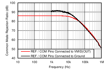
INA1650 INA1651 C303_SBOS818.png
Figure 9. Common-Mode Rejection Ratio vs Frequency
INA1650 INA1651 C304_SBOS818.png
Figure 11. Voltage Noise Spectral Density
INA1650 INA1651 C102_SBOS818.png
3 VRMS, 500-kHz Measurement Bandwidth
Figure 13. THD+N vs Frequency
INA1650 INA1651 C104_SBOS818.png
SMPTE 4:1 60 Hz and 7 kHz, 90-kHz Measurement Bandwidth
Figure 15. SMPTE Intermodulation Distortion vs Output Amplitude
INA1650 INA1651 C207_SBOS818.png
Figure 17. Signal Path Output Impedance vs Frequency
INA1650 INA1651 C305_SBOS818.png
100-mV Input Step
Figure 19. Overshoot vs Capacitive Load
INA1650 INA1651 C307_SBOS818.png
10-mV Input Step
Figure 21. Small-Signal Step Response
INA1650 INA1651 C309_SBOS818.png
10-V Input Step, 0.01% Settling = ± 1 mV
Figure 23. Rising-Edge Settling Time
INA1650 INA1651 C306_SBOS818.png
Figure 25. No Phase Reversal
INA1650 INA1651 C019_SBOS818.png
5 Typical Units
Figure 27. Output Offset Voltage vs Common-Mode Voltage
INA1650 INA1651 C007_SBOS818.png
Figure 29. Positive Output Voltage vs Output Current
INA1650 INA1651 C005_SBOS818.png
Figure 31. Power Supply Current vs Power Supply Voltage
INA1650 INA1651 ai_C006_SBOS818.png
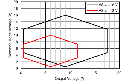
REF A/B connected to 0 V
Figure 33. Input Common-Mode Voltage vs Output Voltage
INA1650 INA1651 ai_C008_SBOS818.png
REF A/B connected to VMID(OUT)
Figure 35. Input Common-Mode Voltage vs Output Voltage
INA1650 INA1651 ai_C010_SBOS818.png
REF A/B connected to 0 V
Figure 37. Input Common-Mode Voltage vs Output Voltage
INA1650 INA1651 C109_SBOS818.png
5746 Channels
VREF Pins Connected to VMID(OUT)
Figure 2. Common-Mode Rejection Ratio Distribution
INA1650 INA1651 C111_SBOS818.png
5746 Channels
Figure 4. Gain Error Distribution
INA1650 INA1651 C009_SBOS818.png
52 Channels
Figure 6. Offset Voltage Drift Distribution
INA1650 INA1651 ai_C012_OPA1678.png
Figure 8. Maximum Output Voltage vs Frequency
INA1650 INA1651 C302_SBOS818.png
Figure 10. Power Supply Rejection Ratio vs Frequency
INA1650 INA1651 C101_SBOS818.png
3 VRMS, 90-kHz Measurement Bandwidth
Figure 12. THD+N vs Frequency
INA1650 INA1651 C103_SBOS818.png
1 kHz, 90-kHz Measurement Bandwidth
Figure 14. THD+N vs Output Amplitude
INA1650 INA1651 C105_SBOS818.png
CCIF 19 kHz and 20 kHz, 90-kHz Measurement Bandwidth
Figure 16. CCIF Intermodulation Distortion vs Output Amplitude
INA1650 INA1651 C208_SBOS818.png
CF = 1 µF
Figure 18. Supply Divider Output Impedance vs Frequency
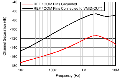
INA1650 INA1651 C210_SBOS818.png
Figure 20. Channel Separation vs Frequency
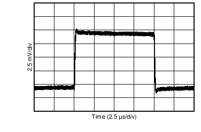
INA1650 INA1651 C308_SBOS818.png
10-V Input Step
Figure 22. Large-Signal Step Response
INA1650 INA1651 C310_SBOS818.png
10-V Input Step, 0.01% Settling = ± 1 mV
Figure 24. Falling-Edge Settling Time
INA1650 INA1651 C017_SBOS818.png
5 Typical Units
Figure 26. CMRR vs Temperature
INA1650 INA1651 C006_SBOS818.png
Figure 28. Short-Circuit Current vs Temperature
INA1650 INA1651 C907_SBOS818.png
Figure 30. Negative Output Voltage vs Output Current
INA1650 INA1651 C004_SBOS818.png
Figure 32. Power Supply Current vs Temperature
INA1650 INA1651 ai_C007_SBOS818.png
REF A/B connected to 0 V
Figure 34. Input Common-Mode Voltage vs Output Voltage
INA1650 INA1651 ai_C009_SBOS818.png
REF A/B connected to VMID(OUT)
Figure 36. Input Common-Mode Voltage vs Output Voltage
INA1650 INA1651 ai_C011_SBOS818.png
REF A/B connected to 0 V
Figure 38. Input Common-Mode Voltage vs Output Voltage