-
INA1x8 High-Side Measurement Current Shunt Monitor
- 1 Features
- 2 Applications
- 3 Description
- 4 Revision History
- 5 Pin Configuration and Functions
- 6 Specifications
- 7 Detailed Description
-
8 Application and Implementation
- 8.1 Application Information
- 8.2 Typical Applications
- 9 Power Supply Recommendations
- 10Layout
- 11Device and Documentation Support
- 12Mechanical, Packaging, and Orderable Information
- IMPORTANT NOTICE
Package Options
Mechanical Data (Package|Pins)
- DBV|5
Thermal pad, mechanical data (Package|Pins)
Orderable Information
INA1x8 High-Side Measurement Current Shunt Monitor
1 Features
- Complete Unipolar High-Side Current Measurement Circuit
- Wide Supply and Common-Mode Range
- INA138: 2.7 V to 36 V
- INA168: 2.7 V to 60 V
- Independent Supply and Input Common-Mode Voltages
- Single Resistor Gain Set
- Low Quiescent Current (25 µA Typical)
- Wide Temperature Range: –40°C to +125°C
- 5-Pin SOT-23 Package
2 Applications
- Current Shunt Measurement:
- Telephone, Computers
- Portable and Battery-Backup Systems
- Battery Chargers
- Power Management
- Cell Phones
- Precision Current Source
3 Description
The INA138 and INA168 (INA1x8) are high-side, unipolar, current shunt monitors. Wide input common-mode voltage range, low quiescent current, and tiny SOT-23 packaging enable use in a variety of applications.
Input common-mode and power-supply voltages are independent and can range from 2.7 V to 36 V for the INA138 and 2.7 V to 60 V for the INA168. Quiescent current is only 25 µA, which permits connecting the power supply to either side of the current measurement shunt with minimal error.
The device converts a differential input voltage to a current output. This current is converted back to a voltage with an external load resistor that sets any gain from 1 to over 100. Although designed for current shunt measurement, the circuit invites creative applications in measurement and level shifting.
Both the INA138 and INA168 are available in SOT23-5 and are specified for the –40°C to 125°C temperature range.
Device Information(1)
| PART NUMBER | PACKAGE | BODY SIZE (NOM) |
|---|---|---|
| INA138 | SOT-23 (5) | 2.90 mm × 1.60 mm |
| INA168 |
- For all available packages, see the package option addendum at the end of the datasheet.
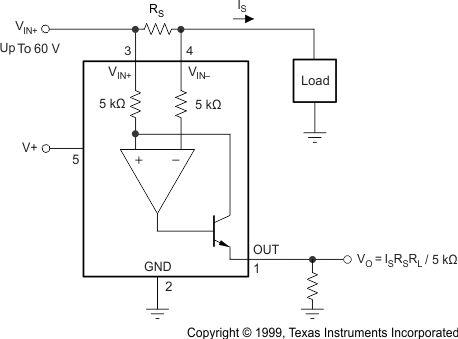
Typical Application Circuit
4 Revision History
Changes from D Revision (December 2014) to E Revision
- Added reference design link to navigation bar at the top of the front pageGo
- Changed body size from 18.00 mm × 18.00 mm to 2.90 mm × 1.60 mm in Device Information tableGo
- Changed pin numbers in pin functions table to match pin configuration figureGo
- Changed Absolute Maximum Ratings table for clarity; no values were changed Go
- Changed Recommended Operating Conditions table; moved some content from Electrical Characteristics table, but no values changedGo
- Changed all values in Thermal Information tableGo
- Changed Electrical Characteristics table; reformatted for clarity; moved some content to Recommended Operating Conditions table, and deleted duplicate contentGo
- Changed common-mode rejection test conditions to better highlight each device in Electrical Characteristics table Go
- Changed offset voltage vs temperature to offset voltage drift in Electrical Characteristics tableGo
- Changed offset voltage vs power supply test conditions to better highlight each device in Electrical Characteristics tableGo
- Changed reference in text from Figure 10 to Figure 11 in last paragraph of Selecting the Shunt Resistor and RL sectionGo
Changes from C Revision (November 2005) to D Revision
- Added ESD Ratings table, Feature Description section, Device Functional Modes, Application and Implementation section, Power Supply Recommendations section, Layout section, Device and Documentation Support section, and Mechanical, Packaging, and Orderable Information section. Go
6 Specifications
6.1 Absolute Maximum Ratings
over operating free-air temperature range (unless otherwise noted) (1)| MIN | MAX | UNIT | ||||
|---|---|---|---|---|---|---|
| Voltage | Supply, V+ | INA138 | –0.3 | 60 | V | |
| INA168 | –0.3 | 75 | ||||
| Analog input, VIN+, VIN– | INA138 | Common mode(2) | –0.3 | 60 | ||
| Sense voltage, VSENSE = (VIN+ – VIN–) | –40 | 2 | ||||
| INA168 | Common mode(2) | –0.3 | 75 | |||
| Sense voltage, VSENSE = (VIN+ – VIN–) | –40 | 2 | ||||
| Analog output, OUT pin(2) | –0.3 | 40 | ||||
| Current | Input current into any pin | 10 | mA | |||
| Temperature | Operating, TA | –55 | 150 | °C | ||
| Junction, TJ | 150 | |||||
| Storage, Tstg | –65 | 150 | ||||
6.2 ESD Ratings
| VALUE | UNIT | |||
|---|---|---|---|---|
| V(ESD) | Electrostatic discharge | Human-body model (HBM), per ANSI/ESDA/JEDEC JS-001(1) | ±1000 | V |
| Charged-device model (CDM), per JEDEC specification JESD22-C101(2) | ±500 | |||
6.3 Recommended Operating Conditions
over operating free-air temperature range (unless otherwise noted)6.4 Thermal Information
| THERMAL METRIC(1) | INA1x8 | UNIT | |
|---|---|---|---|
| DBV | |||
| 5 PINS | |||
| RθJA | Junction-to-ambient thermal resistance | 168.3 | °C/W |
| RθJC(top) | Junction-to-case (top) thermal resistance | 73.8 | °C/W |
| RθJB | Junction-to-board thermal resistance | 28.1 | °C/W |
| ψJT | Junction-to-top characterization parameter | 2.5 | °C/W |
| ψJB | Junction-to-board characterization parameter | 27.6 | °C/W |
6.5 Electrical Characteristics
all other characteristics at TA = +25°C, VS = 5 V, VIN+ = 12 V, and ROUT = 125 kΩ (unless otherwise noted)| PARAMETER | TEST CONDITIONS | INA1x8 | UNIT | ||||
|---|---|---|---|---|---|---|---|
| MIN | TYP | MAX | |||||
| INPUT | |||||||
| Common-mode rejection | VSENSE = 50 mV | INA138, VIN+ = 2.7 V to 36 V | 100 | 120 | dB | ||
| INA168, VIN+ = 2.7 V to 60 V | 100 | 120 | |||||
| Offset voltage(1) | TA = 25°C | ±0.2 | ±1 | mV | |||
| TA = –40°C to +125°C | ±2 | ||||||
| Offset voltage drift(1) | TA = –40°C to +125°C | 1 | µV/°C | ||||
| Offset voltage vs power supply, V+ | VSENSE = 50 mV | INA138, V+ = 2.7 V to 36 V | 0.1 | 10 | µV/V | ||
| INA168, V+ = 2.7 V to 60 V | 0.1 | 10 | |||||
| Input bias current | TA = 25°C | 2 | µA | ||||
| TA = –40°C to +125°C, INA138 | 10 | ||||||
| OUTPUT | |||||||
| Transconductance | VSENSE = 10 mV to 150 mV, TA = 25°C | 198 | 200 | 202 | µA/V | ||
| VSENSE = 100 mV, TA = –40°C to +125°C | 196 | 204 | µA/V | ||||
| Transconductance drift | TA = –40°C to +125°C | 10 | nA/°C | ||||
| Nonlinearity error | VSENSE = 10 mV to 150 mV | ±0.01% | ±0.1% | ||||
| Total output error | VSENSE = 100 mV | TA = 25°C | ±0.5% | ±2% | |||
| TA = –40°C to +125°C | ±2.5% | ||||||
| Output impedance | 1 || 5 | GΩ || pF | |||||
| Voltage output swing | To power supply voltage, V+ | (V+) – 0.8 | (V+) – 1.0 | V | |||
| To common-mode voltage, VCM | VCM – 0.5 | VCM – 0.8 | V | ||||
| FREQUENCY RESPONSE | |||||||
| Bandwidth | ROUT = 5 kΩ | 800 | kHz | ||||
| ROUT = 125 kΩ | 32 | kHz | |||||
| Settling time | To 0.1% | 5-V step, ROUT = 5 kΩ | 1.8 | µs | |||
| 5-V step, ROUT = 125 kΩ | 30 | µs | |||||
| NOISE | |||||||
| Output-current noise density | 9 | pA/√Hz | |||||
| Total output-current noise | BW = 100 kHz | 3 | nA RMS | ||||
| POWER SUPPLY | |||||||
| Quiescent current | VSENSE = 0 V, IO = 0 mA |
TA = 25°C | 25 | 45 | µA | ||
| TA = –40°C to +125°C | 60 | µA | |||||
6.6 Typical Characteristics
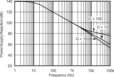
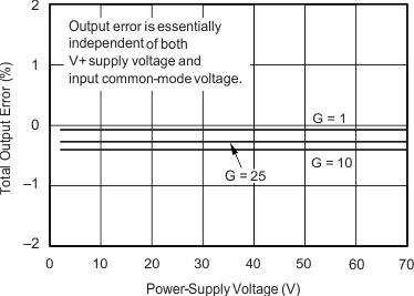
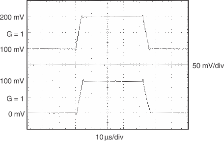
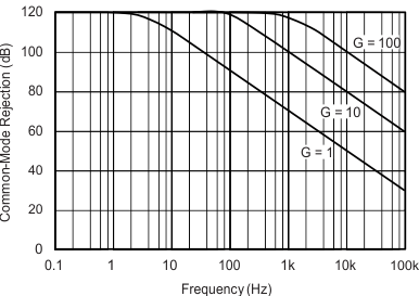
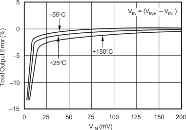
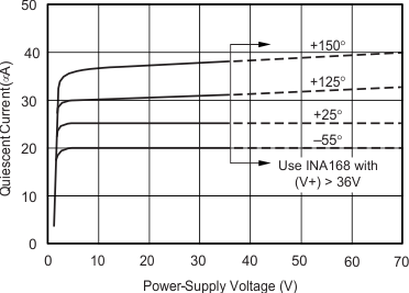
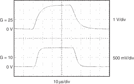
At TA = +25°C, V+ = 5 V, VIN+ = 12 V, and RL = 125 kΩ, unless otherwise noted.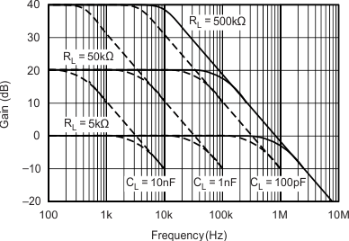
7 Detailed Description
7.1 Overview
The INA138 and INA168 devices (INA1x8) are comprised of a high voltage, precision operational amplifier, precision thin film resistors trimmed in production to an absolute tolerance and a low noise output transistor. The INA1x8 devices can be powered from a single power supply and their input voltages can exceed the power supply voltage. The INA1x8 devices are ideal for measuring small differential voltages, such as those generated across a shunt resistor, in the presence of large common-mode voltages. Refer to Functional Block Diagram which illustrates the functional components within both INA1x8 devices.
7.2 Functional Block Diagram

7.3 Feature Description
7.3.1 Output Voltage Range
The output of the INA1x8 device is a current that is converted to a voltage by the load resistor, RL. The output current remains accurate within the compliance voltage range of the output circuitry. The shunt voltage and the input common-mode and power-supply voltages limit the maximum possible output swing. The maximum output voltage (Vout max) compliance is limited by either Equation 1 or Equation 2, whichever is lower:
or
7.3.2 Bandwidth
Measurement bandwidth is affected by the value of the load resistor, RL. High gain produced by high values of RL will yield a narrower measurement bandwidth (see Typical Characteristics). For widest possible bandwidth, keep the capacitive load on the output to a minimum. Reduction in bandwidth due to capacitive load is shown in the Typical Characteristics.
If bandwidth limiting (filtering) is desired, a capacitor can be added to the output (see Figure 12). This will not cause instability.
7.4 Device Functional Modes
For proper operation the INA1x8 devices must operate within their specified limits. Operating either device outside of their specified power supply voltage range or their specified common-mode range will result in unexpected behavior and is not recommended. Additionally operating the output beyond their specified limits with respect to power supply voltage and input common-mode voltage will also produce unexpected results. Refer to Electrical Characteristics for the device specifications.
8 Application and Implementation
NOTE
Information in the following applications sections is not part of the TI component specification, and TI does not warrant its accuracy or completeness. TI’s customers are responsible for determining suitability of components for their purposes. Customers should validate and test their design implementation to confirm system functionality.
8.1 Application Information
8.1.1 Operation
Figure 9 illustrates the basic circuit diagram for both the INA138 and INA168 devices. Load current IS is drawn from supply VS through shunt resistor RS. The voltage drop in shunt resistor VS is forced across RG1 by the internal op amp, causing current to flow into the collector of Q1. External resistor RL converts the output current to a voltage, VOUT, at the OUT pin. The transfer function for the INA138 device is:
where gm = 200 µA/V.
In the circuit of Figure 9, the input voltage, (VIN+ – VIN–), is equal to IS × RS and the output voltage, VOUT, is equal to IO × RL. The transconductance, gm, of the INA138 device is 200 µA/V. The complete transfer function for the current measurement amplifier in this application is:
The maximum differential input voltage for accurate measurements is 0.5 V, which produces a 100-µA output current. A differential input voltage of up to 2 V will not cause damage. Differential measurements (pins 3 and 4) must be unipolar with a more-positive voltage applied to pin 3. If a more-negative voltage is applied to pin 3, the output current, IO, will be zero, but it will not cause damage.

8.2 Typical Applications
The INA1x8 devices are designed for current shunt measurement circuits, as shown in Figure 9, but basic device function is useful in a wide range of circuitry. A creative engineer will find many unforeseen uses in measurement and level-shifting circuits. A few ideas are illustrated in Figure 10 through Figure 18.
8.2.1 Buffering Output to Drive an ADC
 Figure 10. Buffering Output to Drive an ADC
8.2.1.1 Design Requirements
Digitize the output of the INA1x8 devices using a 1-MSPS analog-to-digital converter (ADC).
8.2.1.2 Detailed Design Procedure
8.2.1.2.1 Selecting the Shunt Resistor and RL
In Figure 9 the value chosen for the shunt resistor depends on the application and is a compromise between small-signal accuracy and maximum permissible voltage loss in the measurement line. High values of shunt resistor provide better accuracy at lower currents by minimizing the effects of offset, while low values of shunt resistor minimize voltage loss in the supply line. For most applications, best performance is attained with a shunt resistor value that provides a full-scale shunt voltage range of 50 mV to 100 mV. Maximum input voltage for accurate measurements is 500 mV.
The load resistor, RL, is chosen to provide the desired full-scale output voltage. The output impedance of the INA1x8 OUT terminal is very high which permits using values of RL up to 500 kΩ with excellent accuracy. The input impedance of any additional circuitry at the output should be much higher than the value of RL to avoid degrading accuracy.
Some analog-to-digital converters (ADCs) have input impedances that significantly affect measurement gain. The input impedance of the ADC can be included as part of the effective RL if its input can be modeled as a resistor to ground. Alternatively, an op amp can be used to buffer the ADC input. The INA1x8 are current output devices, and as such have an inherently large output impedance. The output currents from the amplifier are converted to an output voltage via the load resistor, RL, connected from the amplifier output to ground. The ratio of the load resistor value to that of the internal resistor value determines the voltage gain of the system.
In many applications digitizing the output of the INA1x8 device is required, and can be accomplished by connecting the output of the amplifier to an ADC. It is very common for an ADC to have a dynamic input impedance. If the INA1x8 output is connected directly to an ADC input, the input impedance of the ADC is effectively connected in parallel with the gain setting resistor RL. This parallel impedance combination will affect the gain of the system and the impact on the gain is difficult to estimate accurately. A simple solution that eliminates the paralleling of impedances, simplifying the gain of the circuit is to place a buffer amplifier, such as the OPA340, between the output of the INA138 or INA168 device and the input to the ADC.
Figure 10 illustrates this concept. Notice that a low pass filter is placed between the OPA340 output and the input to the ADC. The filter capacitor is required to provide any instantaneous demand for current required by the input stage of the ADC. The filter resistor is required to isolate the OPA340 output from the filter capacitor to maintain circuit stability. The values for the filter components will vary according to the operational amplifier used for the buffer and the particular ADC selected. More information can be found regarding the design of the low pass filter in the TI Precision Design , 16 bit 1MSPS Data Acquisition Reference Design for Single-Ended Multiplexed Applications (TIPD173).
Figure 11 shows the expected results when driving an analog-to-digital converter at 1MSPS with and without buffering the INA1x8 output. Without the buffer, the high impedance of the INA1x8 reacts with the input capacitance and sample and hold (S/H) capacitance of the ADC, and does not allow the S/H to reach the correct final value before it is reset and the next conversion starts. Adding the buffer amplifier significantly reduces the output impedance driving the S/H and allows for higher conversion rates than can be achieved without adding the buffer.
8.2.1.3 Application Curve
 Figure 11. Driving an ADC With and Without a Buffer
8.2.2 Output Filter
 Figure 12. Output Filter
8.2.2.1 Design Requirements
Filter the output of the INA1x8 devices.
8.2.2.2 Detailed Design Procedure
A low-pass filter can be formed at the output of the INA1x8 devices simply by placing a capacitor of the desired value in parallel with the load resistor. First determine the value of the load resistor needed to achieve the desired gain. Refer to the table in Figure 9. Next, determine the capacitor value that will result in the desired cutoff frequency according to the equation shown in Figure 12. Figure 13 illustrates various combinations of gain settings (determined by RL) and filter capacitors.
8.2.2.3 Application Curve
 Figure 13. Gain vs Frequency
8.2.3 Offsetting the Output Voltage
For many applications using only a single power supply it may be required to level shift the output voltage away from ground when there is no load current flowing in the shunt resistor. Level shifting the output of the INA1x8 devices is easily accomplished by one of two simple methods shown in Figure 14. The method on the left hand side of Figure 14 illustrates a simple voltage divider method. This method is useful for applications that require the output of the INA1x8 devices to remain centered with respect to the power supply at zero load current through the shunt resistor. Using this method the gain is determine by the parallel combination of R1 and R2 while the output offset is determined by the voltage divider ratio R1 and R2. For applications that may require a fixed value of output offset, independent of the power supply voltage, the current source method shown on the right-hand side of Figure 14 is recommended. With this method a REF200 constant current source is used to generate a constant output offset. Using his method the gain is determined by RL and the offset is determined by the product of the value of the current source and RL.
 Figure 14. Offsetting the Output Voltage
8.2.4 Bipolar Current Measurement
The INA1x8 devices can be configured as shown in Figure 15 in applications where measuring current bi-directionally is required. Two INA devices are required connecting their inputs across the shunt resistor as shown in Figure 15. A comparator, such as the TLV3201, is used to detect the polarity of the load current. The magnitude of the load current is monitored across the resistor connected between ground and the connection labeled Output. In this example the 100-kΩ resistor results in a gain of 20 V/V. The 10-kΩ resistors connected in series with the INA1x8 output current are used to develop a voltage across the comparator inputs. Two diodes are required to prevent current flow into the INA1x8 output, as only one device at a time is providing current to the Output connection of the circuit. The circuit functionality is illustrated in Figure 16.
 Figure 15. Bipolar Current Measurement
 Figure 16. Bipolar Current Measurements Results (arbitrary scale)
8.2.5 Bipolar Current Measurement Using Differential Input of ADC
The INA1x8 devices can be used with an ADC such as the ADS7870 programmed for differential mode operation. Figure 17 illustrates this configuration. In this configuration the use of two INAs allows for bidirectional current measurement. Depending upon the polarity of the current, one of the INAs provides an output voltage, while the other output is zero. In this way the ADC reads the polarity of current directly, without the need for additional circuitry.
 Figure 17. Bipolar Current Measurement Using Differential Input of ADC
8.2.6 Multiplexed Measurement Using Logic Signal for Power
Multiple loads can be measured as illustrated in Figure 18. In this configuration each INA1x8 device is powered by the digital I/O from the ADS7870. Multiplexing is achieved by switching on or off each the desired I/O.
 Figure 18. Multiplexed Measurement Using Logic Signal for Power
9 Power Supply Recommendations
The input circuitry of the INA138 can accurately measure beyond its power-supply voltage, V+. For example, the V+ power supply can be 5 V, whereas the load power supply voltage is up to 36 V (or 60 V with the INA168). The output voltage range of the OUT terminal, however, is limited by the lesser of the two voltages (see Output Voltage Range). A 0.1-µF capacitor is recommenced to be placed near the power supply pin on the INA138 or INA168. Additional capacitance may be required for applications with noisy power supply voltages.
10 Layout
10.1 Layout Guidelines
Figure 19 shows the basic connection of the INA138 device. The input pins, VIN+ and VIN– , should be connected as closely as possible to the shunt resistor to minimize any resistance in series with the shunt resistance. The output resistor, RL, is shown connected between pin 1 and ground. Best accuracy is achieved with the output voltage measured directly across RL. This is especially important in high-current systems where load current could flow in the ground connections, affecting the measurement accuracy.
No power-supply bypass capacitors are required for stability of the INA138. However, applications with noisy or high-impedance power supplies may require decoupling capacitors to reject power-supply noise. Connect bypass capacitors close to the device pins.
10.2 Layout Example
 Figure 19. Typical Layout Example
11 Device and Documentation Support
11.1 Documentation Support
11.1.1 Related Documentation
For related documentation see the following:
11.2 Related Links
Table 1 lists quick access links. Categories include technical documents, support and community resources, tools and software, and quick access to sample or buy.
Table 1. Related Links
| PARTS | PRODUCT FOLDER | SAMPLE & BUY | TECHNICAL DOCUMENTS | TOOLS & SOFTWARE | SUPPORT & COMMUNITY |
|---|---|---|---|---|---|
| INA138 | Click here | Click here | Click here | Click here | Click here |
| INA168 | Click here | Click here | Click here | Click here | Click here |
11.3 Receiving Notification of Documentation Updates
To receive notification of documentation updates, navigate to the device product folder on ti.com. In the upper right corner, click on Alert me to register and receive a weekly digest of any product information that has changed. For change details, review the revision history included in any revised document.
11.4 Community Resources
The following links connect to TI community resources. Linked contents are provided "AS IS" by the respective contributors. They do not constitute TI specifications and do not necessarily reflect TI's views; see TI's Terms of Use.
-
TI E2E™ Online Community TI's Engineer-to-Engineer (E2E) Community. Created to foster collaboration among engineers. At e2e.ti.com, you can ask questions, share knowledge, explore ideas and help solve problems with fellow engineers.
-
Design Support TI's Design Support Quickly find helpful E2E forums along with design support tools and contact information for technical support.
11.5 Trademarks
E2E is a trademark of Texas Instruments.
All other trademarks are the property of their respective owners.
11.6 Electrostatic Discharge Caution

This integrated circuit can be damaged by ESD. Texas Instruments recommends that all integrated circuits be handled with appropriate precautions. Failure to observe proper handling and installation procedures can cause damage.
ESD damage can range from subtle performance degradation to complete device failure. Precision integrated circuits may be more susceptible to damage because very small parametric changes could cause the device not to meet its published specifications.
11.7 Glossary
SLYZ022 — TI Glossary.
This glossary lists and explains terms, acronyms, and definitions.
12 Mechanical, Packaging, and Orderable Information
The following pages include mechanical, packaging, and orderable information. This information is the most current data available for the designated devices. This data is subject to change without notice and revision of this document. For browser-based versions of this data sheet, refer to the left-hand navigation.
IMPORTANT NOTICE
Texas Instruments Incorporated (TI) reserves the right to make corrections, enhancements, improvements and other changes to its semiconductor products and services per JESD46, latest issue, and to discontinue any product or service per JESD48, latest issue. Buyers should obtain the latest relevant information before placing orders and should verify that such information is current and complete.
TI’s published terms of sale for semiconductor products (http://www.ti.com/sc/docs/stdterms.htm) apply to the sale of packaged integrated circuit products that TI has qualified and released to market. Additional terms may apply to the use or sale of other types of TI products and services.
Reproduction of significant portions of TI information in TI data sheets is permissible only if reproduction is without alteration and is accompanied by all associated warranties, conditions, limitations, and notices. TI is not responsible or liable for such reproduced documentation. Information of third parties may be subject to additional restrictions. Resale of TI products or services with statements different from or beyond the parameters stated by TI for that product or service voids all express and any implied warranties for the associated TI product or service and is an unfair and deceptive business practice. TI is not responsible or liable for any such statements.
Buyers and others who are developing systems that incorporate TI products (collectively, “Designers”) understand and agrees that Designers remain responsible for using their independent analysis, evaluation and judgment in designing their systems and products, and have full and exclusive responsibility to assure the safety of their products and compliance of their products (and of all TI products used in or for such Designers’ products) with all applicable regulations, laws and other applicable requirements. Designers represent that, with respect to their applications, they have all the necessary expertise to create and implement safeguards that (1) anticipate dangerous consequences of failures, (2) monitor failures and their consequences, and (3) lessen the likelihood of failures that might cause harm and take appropriate actions. Designers agree that prior to using or distributing any systems that include TI products, they will thoroughly test such systems and the functionality of such TI products as used in such systems.
TI’s provision of reference designs and any other technical, applications or design advice, quality characterization, reliability data or other information or services does not expand or otherwise alter TI’s applicable published warranties or warranty disclaimers for TI products, and no additional obligations or liabilities arise from TI providing such reference designs or other items.
Designers are authorized to use, copy and modify any individual TI reference design only in connection with the development of end products that include the TI product(s) identified in that reference design. HOWEVER, NO OTHER LICENSE, EXPRESS OR IMPLIED, BY ESTOPPEL OR OTHERWISE TO ANY OTHER TI INTELLECTUAL PROPERTY RIGHT, AND NO LICENSE TO ANY TECHNOLOGY OR INTELLECTUAL PROPERTY RIGHT OF TI OR ANY THIRD PARTY IS GRANTED HEREIN, including but not limited to any patent right, copyright, mask work right, or other intellectual property right relating to any combination, machine, or process in which TI products or services are used. Information published by TI regarding third-party products or services does not constitute a license to use such products or services, or a warranty or endorsement thereof. Use of the reference design or other items described above may require a license from a third party under the patents or other intellectual property of the third party, or a license from TI under the patents or other intellectual property of TI.
TI REFERENCE DESIGNS AND OTHER ITEMS DESCRIBED ABOVE ARE PROVIDED “AS IS” AND WITH ALL FAULTS. TI DISCLAIMS ALL OTHER WARRANTIES OR REPRESENTATIONS, EXPRESS OR IMPLIED, REGARDING THE REFERENCE DESIGNS OR USE OF THE REFERENCE DESIGNS, INCLUDING BUT NOT LIMITED TO ACCURACY OR COMPLETENESS, TITLE, ANY EPIDEMIC FAILURE WARRANTY AND ANY IMPLIED WARRANTIES OF MERCHANTABILITY, FITNESS FOR A PARTICULAR PURPOSE, AND NON-INFRINGEMENT OF ANY THIRD PARTY INTELLECTUAL PROPERTY RIGHTS.
TI SHALL NOT BE LIABLE FOR AND SHALL NOT DEFEND OR INDEMNIFY DESIGNERS AGAINST ANY CLAIM, INCLUDING BUT NOT LIMITED TO ANY INFRINGEMENT CLAIM THAT RELATES TO OR IS BASED ON ANY COMBINATION OF PRODUCTS AS DESCRIBED IN A TI REFERENCE DESIGN OR OTHERWISE. IN NO EVENT SHALL TI BE LIABLE FOR ANY ACTUAL, DIRECT, SPECIAL, COLLATERAL, INDIRECT, PUNITIVE, INCIDENTAL, CONSEQUENTIAL OR EXEMPLARY DAMAGES IN CONNECTION WITH OR ARISING OUT OF THE REFERENCE DESIGNS OR USE OF THE REFERENCE DESIGNS, AND REGARDLESS OF WHETHER TI HAS BEEN ADVISED OF THE POSSIBILITY OF SUCH DAMAGES.
Unless TI has explicitly designated an individual product as meeting the requirements of a particular industry standard (e.g., ISO/TS 16949 and ISO 26262), TI is not responsible for any failure to meet such industry standard requirements.
Where TI specifically promotes products as facilitating functional safety or as compliant with industry functional safety standards, such products are intended to help enable customers to design and create their own applications that meet applicable functional safety standards and requirements. Using products in an application does not by itself establish any safety features in the application. Designers must ensure compliance with safety-related requirements and standards applicable to their applications. Designer may not use any TI products in life-critical medical equipment unless authorized officers of the parties have executed a special contract specifically governing such use. Life-critical medical equipment is medical equipment where failure of such equipment would cause serious bodily injury or death (e.g., life support, pacemakers, defibrillators, heart pumps, neurostimulators, and implantables). Such equipment includes, without limitation, all medical devices identified by the U.S. Food and Drug Administration as Class III devices and equivalent classifications outside the U.S.
TI may expressly designate certain products as completing a particular qualification (e.g., Q100, Military Grade, or Enhanced Product). Designers agree that it has the necessary expertise to select the product with the appropriate qualification designation for their applications and that proper product selection is at Designers’ own risk. Designers are solely responsible for compliance with all legal and regulatory requirements in connection with such selection.
Designer will fully indemnify TI and its representatives against any damages, costs, losses, and/or liabilities arising out of Designer’s non-compliance with the terms and provisions of this Notice.
IMPORTANT NOTICE
| Mailing Address: Texas Instruments, Post Office Box 655303, Dallas, Texas 75265 Copyright © 2017, Texas Instruments Incorporated |