performance measured with the INA199B3-Q1 at TA = 25°C, VS = 5 V, VIN+ = 12 V, and VREF = VS / 2 (unless otherwise noted)
 Figure 7-1 Offset Voltage vs. Temperature
| VCM = 0 V,
VDIF = 15-mVPP sine |
|

| VS = 5 V, VCM = 1-V sine, VDIF = shorted, VREF = 2.5 V |
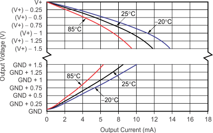
 Figure 7-7 Output Voltage Swing vs. Output Current
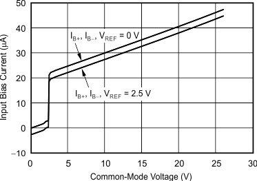
 Figure 7-9 Input Bias Current vs. Common-Mode Voltage With Supply Voltage = 0 V (Shutdown)
 Figure 7-11 Quiescent Current vs. Temperature
| VS = ±2.5 V, VCM = 0 V, VDIF = 0 V, VREF = 0 V |
 Figure 7-15 Common-Mode Voltage Transient Response
| VS = 5 V, VCM = 12 V, VREF = 2.5 V |

| VS = 5 V, 1-kHz step with VDIF = 0 V, VREF = 2.5 V |
 Figure 7-1 Offset Voltage vs. Temperature


 Figure 7-9 Input Bias Current vs. Common-Mode Voltage With Supply Voltage = 0 V (Shutdown)
 Figure 7-11 Quiescent Current vs. Temperature
 Figure 7-15 Common-Mode Voltage Transient Response

 Figure 7-2 Common-Mode Rejection Ratio vs. Temperature
 Figure 7-6 Output Voltage Swing vs. Output Current
 Figure 7-8 Input Bias Current vs. Common-Mode Voltage With Supply Voltage = 5 V
 Figure 7-10 Input Bias Current vs. Temperature
 Figure 7-14 Step Response (10-mVPP Input Step)
