SBOS781E March 2016 – May 2021 INA199-Q1
PRODUCTION DATA
- 1 Features
- 2 Applications
- 3 Description
- 4 Revision History
- 5 Device Comparison
- 6 Pin Configuration and Functions
- 7 Specifications
- 8 Detailed Description
- 9 Application and Implementation
- 10Power Supply Recommendations
- 11Layout
- 12Device and Documentation Support
- 13Mechanical, Packaging, and Orderable Information
Package Options
Mechanical Data (Package|Pins)
- DCK|6
Thermal pad, mechanical data (Package|Pins)
Orderable Information
3 Description
The INA199-Q1 is a voltage-output, current-sense amplifier that can sense drops across shunts at common-mode voltages from –0.1 V to 26V, independent of the supply voltage. Three fixed gains are available: 50V/V, 100V/V, and 200V/V. The low offset of the zero-drift architecture enables current sensing with maximum drops across the shunt as low as 10-mV full-scale.
This device operates from a single 2.7-V to 26-V power supply, drawing a maximum of 100 μA of supply current. All gain options are specified from –40°C to +125°C, and are offered in a 6-pin SC70 package.
Device Information(1)
| PART NUMBER | PACKAGE | BODY SIZE (NOM) |
|---|---|---|
| INA199-Q1 | SC70 (6) | 2.00 mm × 1.25 mm |
(1) For all available packages, see the package option addendum at the end of the data sheet.
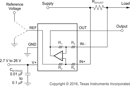
 Simplified Schematic