SBOS360F June 2006 – November 2015 INA206 , INA207 , INA208
PRODUCTION DATA.
- 1 Features
- 2 Applications
- 3 Description
- 4 Revision History
- 5 Device Comparison Table
- 6 Pin Configuration and Functions
-
7 Specifications
- 7.1 Absolute Maximum Ratings
- 7.2 ESD Ratings
- 7.3 Recommended Operating Conditions
- 7.4 Thermal Information
- 7.5 Electrical Characteristics: Current-Shunt Monitor
- 7.6 Electrical Characteristics: Comparator
- 7.7 Electrical Characteristics: Reference
- 7.8 Electrical Characteristics: General
- 7.9 Typical Characteristics
- 8 Detailed Description
- 9 Application and Implementation
- 10Power Supply Recommendations
- 11Layout
- 12Device and Documentation Support
- 13Mechanical, Packaging, and Orderable Information
Package Options
Refer to the PDF data sheet for device specific package drawings
Mechanical Data (Package|Pins)
- D|14
- DGS|10
- PW|14
Thermal pad, mechanical data (Package|Pins)
Orderable Information
9 Application and Implementation
NOTE
Information in the following applications sections is not part of the TI component specification, and TI does not warrant its accuracy or completeness. TI’s customers are responsible for determining suitability of components for their purposes. Customers should validate and test their design implementation to confirm system functionality.
9.1 Application Information
9.1.1 Basic Connection
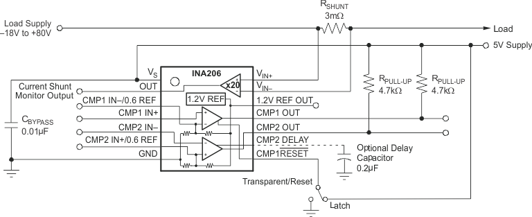
Figure 40 shows the basic connection of the INA206, INA207, and INA208. The input pins, VIN+ and VIN–, should be connected as closely as possible to the shunt resistor to minimize any resistance in series with the shunt resistance.
Power-supply bypass capacitors are required for stability. Applications with noisy or high impedance power supplies may require additional decoupling capacitors to reject power-supply noise. Connect bypass capacitors close to the device pins.
 Figure 40. INA20x Basic Connection
9.2 Typical Application
 Figure 41. Using the INA206, INA207, and INA208 as Window Comparators
9.2.1 Design Requirements
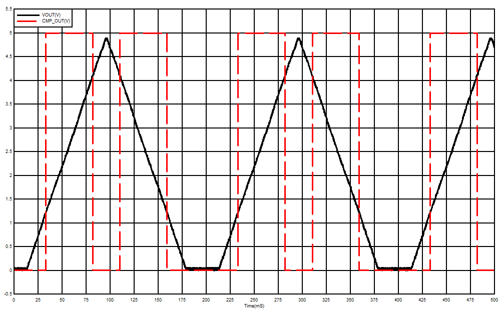
The device measures current through a resistive shunt with current flowing in one direction. The outputs of the two comparators are in logic AND connection thus enabling the window comparison. When the INA output voltage is within the upper and lower limits, the composite comparator output is high. When the INA output voltage is above the upper limit or below the lower limit, the composite comparator output remains low.
9.2.2 Detailed Design Procedure
9.2.2.1 Selecting RS
The value chosen for the shunt resistor, RS, depends on the application and is a compromise between small-signal accuracy and maximum permissible voltage loss in the measurement line. High values of RS provide better accuracy at lower currents by minimizing the effects of offset, while low values of RS minimize voltage loss in the supply line. For most applications, best performance is attained with an RS value that provides a full-scale shunt voltage range of 50 mV to 100 mV. Maximum input voltage for accurate measurements is (VS – 0.2) / Gain.
9.2.2.2 Transient Protection
The –16-V to 80-V common-mode range of the INA206, INA207, and INA208 is ideal for withstanding automotive fault conditions ranging from 12-V battery reversal up to 80-V transients, since no additional protective components are needed up to those levels. In the event that the INA206, INA207, and INA208 are exposed to transients on the inputs in excess of their ratings, then external transient absorption with semiconductor transient absorbers (Zeners or Transzorbs) will be necessary. Use of MOVs or VDRs is not recommended except when they are used in addition to a semiconductor transient absorber. Select the transient absorber such that it will never allow the INA206, INA207, and INA208 to be exposed to transients greater than 80 V (that is, allow for transient absorber tolerance, as well as additional voltage due to transient absorber dynamic impedance). Despite the use of internal Zener-type ESD protection, the INA206, INA207, and INA208 do not lend themselves to using external resistors in series with the inputs since the internal gain resistors can vary up to ±30% but are closely matched. (If gain accuracy is not important, then resistors can be added in series with the INA206, INA207, and INA208 inputs with two equal resistors on each input.)
9.2.2.3 Input Filtering
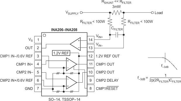
An obvious and straightforward location for filtering is at the output of the INA206, INA207, and INA208 series; however, this location negates the advantage of the low output impedance of the internal buffer. The only other option for filtering is at the input pins of the INA206, INA207, and INA208, which is complicated by the internal 5 kΩ + 30% input impedance; this is shown in Figure 42. Using the lowest possible resistor values minimizes both the initial shift in gain and effects of tolerance. The effect on initial gain is given by Equation 4.

Total effect on gain error can be calculated by replacing the 5-kΩ term with 5 kΩ – 30%, (or 3.5 kΩ) or 5 kΩ + 30%, (or 6.5 kΩ). The tolerance extremes of RFILT can also be inserted into the equation. If a pair of 100 Ω 1% resistors are used on the inputs, the initial gain error will be 1.96%. Worst-case tolerance conditions will always occur at the lower excursion of the internal 5-kΩ resistor (3.5 kΩ), and the higher excursion of RFILT– 2.8% in this case.
 Figure 42. Input Filter (Gain Error 1.5% to 2.8%)
Note that the specified accuracy of the INA26, INA207, and INA208 must then be combined in addition to these tolerances. While this discussion treated accuracy worst-case conditions by combining the extremes of the resistor values, it is appropriate to use geometric mean or root sum square calculations to total the effects of accuracy variations.
9.2.3 Application Curve
 Figure 43. Window Comparator Circuit Response