SBOS475K March 2009 – November 2023 INA210-Q1 , INA211-Q1 , INA212-Q1 , INA213-Q1 , INA214-Q1 , INA215-Q1
PRODUCTION DATA
- 1
- 1 Features
- 2 Applications
- 3 Description
- 4 Pin Configuration and Functions
- 5 Specifications
- 6 Detailed Description
- 7 Application and Implementation
- 8 Power Supply Recommendations
- 9 Layout
- 10Device and Documentation Support
- 11Revision History
- 12Mechanical, Packaging, and Orderable Information
Package Options
Mechanical Data (Package|Pins)
- DCK|6
Thermal pad, mechanical data (Package|Pins)
Orderable Information
3 Description
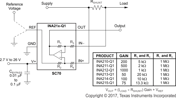
The INA21x-Q1 family of devices is a voltage-output, current-shunt monitor (also called a current-sense amplifier) that can sense drops across shunts at common-mode voltages from –0.3 V to 26 V, independent of the supply voltage. Five fixed gains are available: 50 V/V, 75 V/V, 100 V/V, 200 V/V, 500 V/V, and 1000 V/V. This family of devices is commonly used for overcurrent detection, voltage feedback control loops, or as a power monitor. The low offset of the zero-drift architecture enables current sensing with maximum drops across the shunt as low as 10-mV full-scale.
The devices operate from a single 2.7-V to 26-V power supply, drawing a maximum of 100 µA of supply current. The devices are specified over the operating temperature range of –40°C to +125°C and are offered in a 6-pin SC70 package.
| PART NUMBER | PACKAGE(1) | BODY SIZE (NOM) |
|---|---|---|
| INA210-Q1 | SC70 (6) | 2.00 mm × 1.25 mm |
| INA211-Q1 | SC70 (6) | 2.00 mm × 1.25 mm |
| INA212-Q1 | SC70 (6) | 2.00 mm × 1.25 mm |
| INA213-Q1 | SC70 (6) | 2.00 mm × 1.25 mm |
| INA214-Q1 | SC70 (6) | 2.00 mm × 1.25 mm |
| INA215-Q1 | SC70 (6) | 2.00 mm × 1.25 mm |
 Simplified Schematic