-
INA21x Voltage Output, Low- or High-Side Measurement, Bidirectional, Zero-Drift Series, Current-Shunt Monitors
- 1
- 1 Features
- 2 Applications
- 3 Description
- 4 Pin Configurations and Functions
- 5 Specifications
- 6 Detailed Description
- 7 Application and Implementation
- 8 Power Supply Recommendations
- 9 Layout
- 10Device and Documentation Support
- 11Revision History
- 12Mechanical, Packaging, and Orderable Information
- IMPORTANT NOTICE
Package Options
Mechanical Data (Package|Pins)
Thermal pad, mechanical data (Package|Pins)
Orderable Information
INA21x Voltage Output, Low- or High-Side Measurement, Bidirectional,
Zero-Drift Series, Current-Shunt Monitors
1 Features
Updated format to match new TI layout and flow. Tables, figures and cross-references use a new numbering sequence throughout the document.
Wide Common-Mode Range: –0.3 V to 26 V- Offset Voltage: ±35 μV (Maximum, INA210)
(Enables Shunt Drops of 10-mV Full-Scale) - Accuracy:
- Gain Error (Maximum Over Temperature):
- ±0.5% (Version C)
- ±1% (Versions A and B)
- 0.5-µV/°C Offset Drift (Maximum)
- 10-ppm/°C Gain Drift (Maximum)
- Gain Error (Maximum Over Temperature):
- Choice of Gains:
- INA210: 200 V/V
- INA211: 500 V/V
- INA212: 1000 V/V
- INA213: 50 V/V
- INA214: 100 V/V
- INA215: 75 V/V
- Quiescent Current: 100 μA (Maximum)
- SC70 and Thin UQFN Packages: All Models
2 Applications
- Notebook Computers
- Cell Phones
- Telecom Equipment
- Power Management
- Battery Chargers
3 Description
The INA21x are voltage-output, current-shunt monitors (also called current-sense amplifiers) that are commonly used for overcurrent protection, precision-current measurement for system optimization, or in closed-loop feedback circuits. This series of devices can sense drops across shunts at common-mode voltages from –0.3 V to 26 V, independent of the supply voltage. Six fixed gains are available: 50 V/V, 75 V/V, 100 V/V, 200 V/V, 500 V/V, or 1000 V/V. The low offset of the zero-drift architecture enables current sensing with maximum drops across the shunt as low as 10-mV full-scale.
These devices operate from a single 2.7-V to 26-V
power supply, drawing a maximum of 100 µA of
supply current. All versions are specified over
the extended operating temperature range
(–40°C to +125°C), and
offered in SC70 and UQFN packages.
| PART NUMBER | PACKAGE(1) | BODY SIZE (NOM) |
|---|---|---|
| INA21x | SC70 (6) | 2.00 mm × 1.25 mm |
| UQFN (10) | 1.80 mm × 1.40 mm |
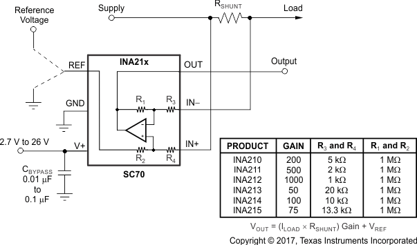
 Simplified Schematic
4 Pin Configurations and Functions
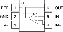
 Figure 4-1 DCK Package6-Pin SC70Top View
| PIN | I/O | DESCRIPTION | ||
|---|---|---|---|---|
| NAME | DCK | RSW | ||
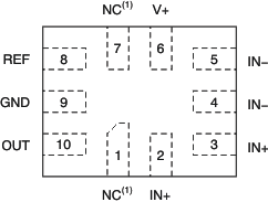
| GND | 2 | 9 | Analog | Ground |
| IN– | 5 | 4, 5 | Analog input | Connect to load side of shunt resistor |
| IN+ | 4 | 2, 3 | Analog input | Connect to supply side of shunt resistor |
| NC | — | 1, 7 | — | Not internally connected. Leave floating or connect to ground. |
| OUT | 6 | 10 | Analog output | Output voltage |
| REF | 1 | 8 | Analog input | Reference voltage, 0 V to V+ |
| V+ | 3 | 6 | Analog | Power supply, 2.7 V to 26 V |
5 Specifications
5.1 Absolute Maximum Ratings
| MIN | MAX | UNIT | ||
|---|---|---|---|---|
| Supply voltage, VS | 26 | V | ||
| Analog inputs, VIN+, VIN–(2) | Differential (VIN+) – (VIN–) | –26 | 26 | V |
| Common-mode (Version A)(3) | GND – 0.3 | 26 | V | |
| Common-mode (Version B)(3) | GND – 0.1 | 26 | V | |
| Common-mode (Version C)(3) | GND – 0.1 | 26 | V | |
| REF input | GND – 0.3 | (VS) + 0.3 | V | |
| Output(3) | GND – 0.3 | (VS) + 0.3 | V | |
| Input current into any terminal(3) | 5 | mA | ||
| Operating temperature | –55 | 150 | °C | |
| Junction temperature | 150 | °C | ||
| Storage temperature, Tstg | –65 | 150 | °C | |
5.2 ESD Ratings
| VALUE | UNIT | |||
|---|---|---|---|---|
| INA21x, (VERSION A) | ||||
| V(ESD) | Electrostatic discharge | Human-body model (HBM), per ANSI/ESDA/JEDEC JS-001(1) | ±2000 | V |
| Charged-device model (CDM), per JEDEC specification JESD22-C101(2) | ±1000 | |||
| INA21x, (VERSIONS B AND C) | ||||
| V(ESD) | Electrostatic discharge | Human-body model (HBM), per ANSI/ESDA/JEDEC JS-001(1) | ±3500 | V |
| Charged-device model (CDM), per JEDEC specification JESD22-C101(2) | ±1000 | |||