SBOS035B december 1995 – may 2023 INA2128
PRODUCTION DATA
- 1
- 1Features
- 2Applications
- 3Description
- 4Revision History
- 5Pin Configuration and Functions
- 6Specifications
- 7Application and Implementation
- 8Device and Documentation Support
- 9Mechanical, Packaging, and Orderable Information
Package Options
Mechanical Data (Package|Pins)
- DW|16
Thermal pad, mechanical data (Package|Pins)
- DW|16
Orderable Information
7.2.8 Input Protection
The inputs of the INA2128 are individually protected for voltages up to ±40 V. For example, a condition of –40 V on one input and +40 V on the other input will not cause damage. Internal circuitry on each input provides low series impedance under normal signal conditions. To provide equivalent protection, series input resistors would contribute excessive noise. If the input is overloaded, the protection circuitry limits the input current to a safe value of approximately 1.5 mA to 5 mA. The typical performance curve “Input Bias Current vs Common-Mode Input Voltage” shows this input current limit behavior. The inputs are protected even if the power supplies are disconnected or turned off.
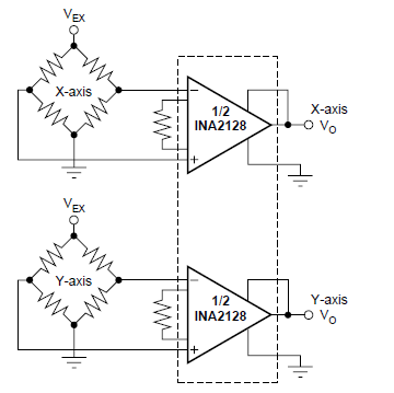
 Figure 7-4 Two-Axis Bridge
Amplifier