SBOS475K March 2009 – November 2023 INA210-Q1 , INA211-Q1 , INA212-Q1 , INA213-Q1 , INA214-Q1 , INA215-Q1
PRODUCTION DATA
- 1
- 1 Features
- 2 Applications
- 3 Description
- 4 Pin Configuration and Functions
- 5 Specifications
- 6 Detailed Description
- 7 Application and Implementation
- 8 Power Supply Recommendations
- 9 Layout
- 10Device and Documentation Support
- 11Revision History
- 12Mechanical, Packaging, and Orderable Information
Package Options
Mechanical Data (Package|Pins)
- DCK|6
Thermal pad, mechanical data (Package|Pins)
Orderable Information
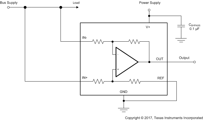
7.2.1 Unidirectional Operation
Unidirectional operation allows the INA21x-Q1 family of devices to measure currents through a resistive shunt in one direction. The most frequent case of unidirectional operation sets the output at ground by connecting the REF pin to ground. In unidirectional applications where the highest possible accuracy is desirable at very low inputs, bias the REF pin to a convenient value above 50 mV to get the device output swing into the linear range for zero inputs.
A less frequent case of unipolar output biasing is to bias the output by connecting the REF pin to the supply. In this case, the quiescent output for zero input is at quiescent supply. This configuration only responds to negative currents (inverted voltage polarity at the device input).
 Figure 7-1 Unidirectional Application Schematic