SBOS247C June 2002 – November 2015 INA217
PRODUCTION DATA.
- 1 Features
- 2 Applications
- 3 Description
- 4 Revision History
- 5 Pin Configuration and Functions
- 6 Specifications
- 7 Detailed Description
- 8 Application and Implementation
- 9 Power Supply Recommendations
- 10Layout
- 11Device and Documentation Support
- 12Mechanical, Packaging, and Orderable Information
Package Options
Mechanical Data (Package|Pins)
- DW|16
Thermal pad, mechanical data (Package|Pins)
- DW|16
Orderable Information
7 Detailed Description
7.1 Overview
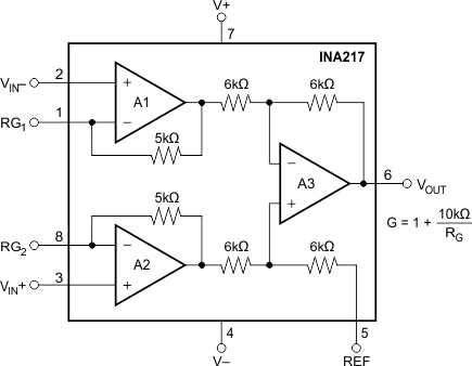
The INA217 is a classical three-amp instrumentation amplifier designed for audio applications. Featuring low noise and low distortion the INA217 is ideally suited for amplifying low level audio signals. With a wide supply voltage, wide output voltage swing, and high output current drive the INA217 is also ideally suited for processing high level audio signals. Specified from –40°C to 85°C the INA217 is well suited for industrial applications.
7.2 Functional Block Diagram

7.3 Feature Description
7.3.1 Basic Connections
Figure 13 shows the basic connections required for operation. Power supplies should be bypassed with 0.1-μF tantalum capacitors near the device pins. The output Reference (pin 5) should be a low-impedance connection. Resistance of a few Ωs in series with this connection will degrade the common-mode rejection of the INA217.
 Figure 13. Basic Circuit Connections
7.3.2 Gain-Set Resistor
Gain is set with an external resistor, RG, as shown in Figure 13. The two internal 5-kΩ feedback resistors are laser-trimmed to 5-kΩ within approximately ±0.2%. Equation 1 shows the gain equation for the INA217.

The temperature coefficient of the internal 5-kΩ resistors is approximately ±25 ppm/°C. Accuracy and TCR of the external RG will also contribute to gain error and temperature drift. These effects can be inferred from the gain equation. Make a short, direct connection to the gain set resistor, RG. Avoid running output signals near these sensitive input nodes.
7.3.3 Noise Performance
The INA217 provides very low noise with low-source impedance. Its 1.3-nV/√Hz voltage noise delivers near-theoretical noise performance with a source impedance of 200 Ω. The input stage design used to achieve this low noise results in relatively high input bias current and input bias current noise. As a result, the INA217 may not provide the best noise performance with a source impedance greater than 10 kΩ. For source impedance greater than 10 kΩ, other instrumentation amplifiers may provide improved noise performance.
7.3.4 Input Considerations
Very low source impedance (less than 10 Ω) can cause the INA217 to oscillate. This depends on circuit layout, signal source, and input cable characteristics. An input network consisting of a small inductor and resistor, as shown in Figure 14, can greatly reduce any tendency to oscillate. This is especially useful if a variety of input sources are to be connected to the INA217. Although not shown in other figures, this network can be used as needed with all applications shown.
 Figure 14. Input Stabilization Network
7.3.5 Offset Voltage Trim
A variable voltage applied to pin 5, as shown in Figure 15, can be used to adjust the output offset voltage. A voltage applied to pin 5 is summed with the output signal. An operational amplifier connected as a buffer is used to provide a low impedance at pin 5 to assure good common-mode rejection.
 Figure 15. Offset Voltage Adjustment Circuit
7.4 Device Functional Modes
The INA217 has a single functional mode of operation. The mode is operational when the power supply voltage exceeds ±4.5 V. The maximum power supply voltage is ±18 V. The INA217 is specified over the temperature range from –40°C to 85°C and is operational to 125°C.