SLYS018F April   2018  – October 2024 INA181-Q1 , INA2181-Q1 , INA4181-Q1

PRODUCTION DATA  

  1.   1
  2. Features
  3. Applications
  4. Description
  5. Device Comparison
  6. Pin Configuration and Functions
  7. Specifications
    1. 6.1 Absolute Maximum Ratings
    2. 6.2 ESD Ratings
    3. 6.3 Recommended Operating Conditions
    4. 6.4 Thermal Information
    5. 6.5 Electrical Characteristics
    6. 6.6 Typical Characteristics
  8. Detailed Description
    1. 7.1 Overview
    2. 7.2 Functional Block Diagrams
    3. 7.3 Feature Description
      1. 7.3.1 High Bandwidth and Slew Rate
      2. 7.3.2 Bidirectional Current Monitoring
      3. 7.3.3 Wide Input Common-Mode Voltage Range
      4. 7.3.4 Precise Low-Side Current Sensing
      5. 7.3.5 Rail-to-Rail Output Swing
    4. 7.4 Device Functional Modes
      1. 7.4.1 Normal Mode
      2. 7.4.2 Unidirectional Mode
      3. 7.4.3 Bidirectional Mode
      4. 7.4.4 Input Differential Overload
      5. 7.4.5 Shutdown Mode
  9. Application and Implementation
    1. 8.1 Application Information
      1. 8.1.1 Basic Connections
      2. 8.1.2 RSENSE and Device Gain Selection
      3. 8.1.3 Signal Filtering
      4. 8.1.4 Summing Multiple Currents
      5. 8.1.5 Detecting Leakage Currents
    2. 8.2 Typical Application
      1. 8.2.1 Design Requirements
      2. 8.2.2 Detailed Design Procedure
      3. 8.2.3 Application Curve
    3. 8.3 Power Supply Recommendations
      1. 8.3.1 Common-Mode Transients Greater Than 26 V
    4. 8.4 Layout
      1. 8.4.1 Layout Guidelines
      2. 8.4.2 Layout Example
  10. Device and Documentation Support
    1. 9.1 Device Support
      1. 9.1.1 Development Support
    2. 9.2 Documentation Support
      1. 9.2.1 Related Documentation
    3. 9.3 Receiving Notification of Documentation Updates
    4. 9.4 Support Resources
    5. 9.5 Trademarks
    6. 9.6 Electrostatic Discharge Caution
    7. 9.7 Glossary
  11. 10Revision History
  12. 11Mechanical, Packaging, and Orderable Information

Package Options

Refer to the PDF data sheet for device specific package drawings

Mechanical Data (Package|Pins)
  • DGS|10
Thermal pad, mechanical data (Package|Pins)
Orderable Information

Summing Multiple Currents

The outputs of the INA2181-Q1 are easily summed by connecting the output of one channel to the reference input of a second channel. The circuit configuration shown in Figure 8-3 is an easy method to achieve current summing. To correctly sum multiple output currents, the values for the current sense resistor RSENSE must be the same for all channels.
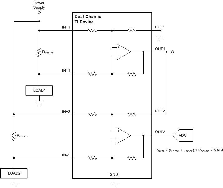
INA181-Q1 INA2181-Q1 INA4181-Q1 Summing Multiple CurrentsFigure 8-3 Summing Multiple Currents

Connect the output of one channel of the INA2181-Q1 to the reference input of the other channel. Use the reference input of the first circuit to set the reference of the final summed output operating point. The currents sensed at each circuit in the chain are summed at the output of the last device in the chain.

An example output response of a summing configuration is shown in Figure 8-4. The reference pin of the first circuit is connected to ground, and sine waves at different frequencies are applied to the two circuits to produce a summed output as shown. The sine wave voltage input for the first circuit is offset so that the whole wave is above GND.
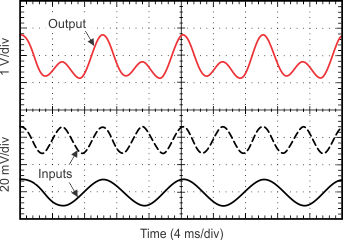
INA181-Q1 INA2181-Q1 INA4181-Q1 Current Summing Application Output Response (A2 Devices)
VREF = 0 V
Figure 8-4 Current Summing Application Output Response (A2 Devices)