SLYS018F April 2018 – October 2024 INA181-Q1 , INA2181-Q1 , INA4181-Q1
PRODUCTION DATA
- 1
- 1 Features
- 2 Applications
- 3 Description
- 4 Device Comparison
- 5 Pin Configuration and Functions
- 6 Specifications
- 7 Detailed Description
- 8 Application and Implementation
- 9 Device and Documentation Support
- 10Revision History
- 11Mechanical, Packaging, and Orderable Information
Package Options
Refer to the PDF data sheet for device specific package drawings
Mechanical Data (Package|Pins)
- DGS|10
Thermal pad, mechanical data (Package|Pins)
Orderable Information
7.3.5 Rail-to-Rail Output Swing
The INAx181-Q1 allow linear current sensing operation with the output close to the supply rail and GND. The maximum specified output swing to the positive rail is 30 mV, and the maximum specified output swing to GND is only 5 mV. To compare the output swing of the INAx181-Q1 to an equivalent operational amplifier (op amp), the inputs are overdriven to approximate the open-loop condition specified in operational amplifier data sheets. The current-sense amplifier is a closed-loop system; therefore, the output swing to GND can be limited by the product of the offset voltage and amplifier gain during unidirectional operation (VREF = 0 V).
For devices that have positive offset voltages, the swing to GND is limited by the larger of either the offset voltage multiplied by the gain or the swing to GND specified in the Electrical Characteristics table.
For example, in an application where the INA181A4-Q1 (gain = 200 V/V) is used for low-side current sensing and the device has an offset of 40 µV, the product of the device offset and gain results in a value of 8 mV, greater than the specified negative swing value. Therefore, the swing to GND for this example is 8 mV. If the same device has an offset of –40 µV, then the calculated zero differential signal is –8 mV. In this case, the offset helps overdrive the swing in the negative direction, and swing performance is consistent with the value specified in the Electrical Characteristics table.
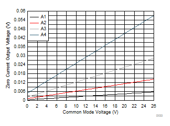
The offset voltage is a function of the common-mode voltage as determined by the CMRR specification; therefore, the offset voltage increases when higher common-mode voltages are present. The increase in offset voltage limits how low the output voltage can go during a zero-current condition when operating at higher common-mode voltages with VREF = 0 V . The typical limitation of the zero-current output voltage vs common-mode voltage for each gain option is shown in Figure 7-5.
 Figure 7-5 Zero-Current Output Voltage vs Common-Mode Voltage