SBOS459E June 2009 – January 2016 INA220
PRODUCTION DATA.
- 1 Features
- 2 Applications
- 3 Description
- 4 Revision History
- 5 Related Products
- 6 Pin Configuration and Functions
- 7 Specifications
-
8 Detailed Description
- 8.1 Overview
- 8.2 Functional Block Diagram
- 8.3 Feature Description
- 8.4 Device Functional Modes
- 8.5 Programming
- 8.6 Register Maps
-
9 Application and Implementation
- 9.1 Application Information
- 9.2 Typical Application
- 10Power Supply Recommendations
- 11Layout
- 12Device and Documentation Support
- 13Mechanical, Packaging, and Orderable Information
Package Options
Mechanical Data (Package|Pins)
- DGS|10
Thermal pad, mechanical data (Package|Pins)
Orderable Information
9 Application and Implementation
NOTE
Information in the following applications sections is not part of the TI component specification, and TI does not warrant its accuracy or completeness. TI’s customers are responsible for determining suitability of components for their purposes. Customers should validate and test their design implementation to confirm system functionality.
9.1 Application Information
The INA220 is a digital current-shunt monitor with an I2C- and SMBus-compatible interface. It provides digital current, voltage, and power readings necessary for accurate decision-making in precisely-controlled systems. Programmable registers allow flexible configuration for measurement resolution, and continuous-versus-triggered operation. See Table 2 for detailed register information. See Figure 29 for a block diagram of the INA220.
9.2 Typical Application
Figure 29 shows a typical application circuit for the INA220. Use a 0.1-μF ceramic capacitor for power-supply bypassing, placed as closely as possible to the supply and ground pins.
The input filter circuit consisting of RF1, RF2, and CF is not necessary in most applications. If the need for filtering is unknown, reserve board space for the components and install 0-Ω resistors unless a filter is needed. See Filtering and Input Considerations.
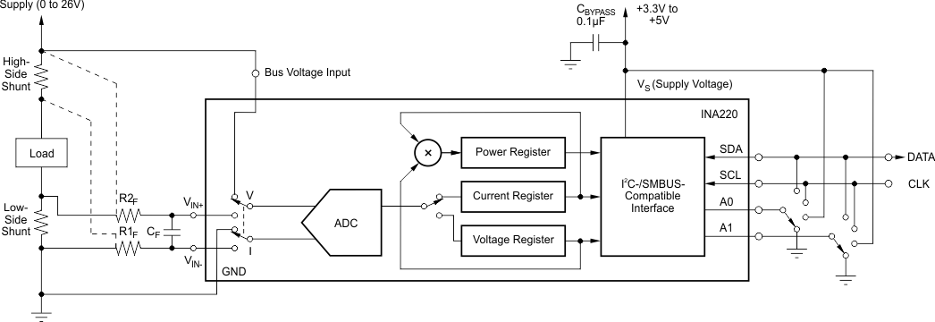 Figure 29. General Load, Low- or High-Side Sensing
9.2.1 Design Requirements
The INA220 measures the voltage across a current-sensing resistor (RSHUNT) when current passes through the resistor. The device also measures the bus supply voltage, and calculates power when calibrated. This section goes through the steps to program the device for power measurements, and shows the register results in Table 7. The Conditions for the example circuit is: Maximum expected load current = 15 A, Nominal load current = 10 A, VCM = 12 V, RSHUNT = 2 mΩ, VSHUNT FSR = 40 mV (PGA = /1), and BRNG = 0 (VBUS range = 16 V).
9.2.2 Detailed Design Procedure
In this example, the 10-A load creates a differential voltage of 20 mV across a 2-mΩ shunt resistor. The voltage present at the IN– pin is equal to the common-mode voltage minus the differential drop across the resistor. The bus voltage for the INA220 is measured at the external VBUS input pin, which in this example is connected to the IN– pin to measure the voltage level delivered to the load. For this example, the voltage at the IN– pin is 11.98 V. For this particular range (40-mV full-scale), this small difference is not a significant deviation from the 12-V common-mode voltage. However, at larger full-scale ranges, this deviation can be much larger.
Note that the Bus Voltage register bits are not right-aligned. To compute the value of the Bus Voltage register contents using the LSB of 4 mV, the register must be shifted right by three bits. This shift puts the BD0 bit in the LSB position so that the contents can be multiplied by the 4-mV LSB value to compute the bus voltage measured by the device. The shifted value of the bus voltage register contents is now equal to BB3h, a decimal equivalent of 2995. This value of 2995 multiplied by the 4-mV LSB results in a value of 11.98 V.
The Calibration register (05h) is set to provide the device information about the current shunt resistor that was used to create the measured shunt voltage. By knowing the value of the shunt resistor, the device can then calculate the amount of current that created the measured shunt voltage drop. The first step when calculating the calibration value is setting the current LSB. The Calibration register value is based on a calculation that has its precision capability limited by the size of the register and the Current register LSB. The device can measure bidirectional current; thus, the MSB of the Current register is a sign bit that allows for the rest of the 15 bits to be used for the Current register value. For this example, the minimum current LSB would be 457.78 µA/bit assuming a maximum expected current of 15 A using Equation 2. For this example, a value of 1 mA/bit was chosen for the current LSB. Setting the current LSB to this value allows for sufficient precision while serving to simplify the math as well. Using Equation 1 results in a Calibration register value of 20480 or 5000h.
The Current register (04h) is internally calculated by multiplying the shunt voltage contents by the Calibration register and then dividing by 4096 using Equation 4. For this example, the shunt voltage of 2000 is multiplied by the Calibration register of 20480 and then divided by 4096 to yield a Current register value of 10000 (2710h).
The Power register (03h) is internally calculated by multiplying the Current register value of 10000 by the Bus Voltage register value of 2995 and then dividing by 5000 using Equation 5. For this example, the Power register contents are 5990 (1766h). Multiplying this result by the power LSB that is 20 times the 1 × 10⁻³ current LSB, or 20 × 10–3, results in a power calculation of 5990 × 20 mW/bit, which equals 119.8 W. This result matches what is expected for this register. A manual calculation for the power being delivered to the load would use 11.98 V
(12 VCM – 20 mV shunt drop) multiplied by the load current of 10 A to give a 119.8-W result.
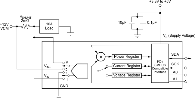 Figure 30. Example Circuit Configuration
9.2.2.1 Register Results for the Example Circuit
Table 7 shows the register readings for the Calibration example.
Table 7. Register Results(1)
| REGISTER NAME | ADDRESS | CONTENTS | ADJ | DEC | LSB | VALUE |
|---|---|---|---|---|---|---|
| Configuration | 00h | 019Fh | ||||
| Shunt | 01h | 07D0h | 2000 | 10 µV | 20 mV | |
| Bus | 02h | 5D98h | 0BB3 | 2995 | 4 mV | 11.98 V |
| Calibration | 05h | 5000h | 20480 | |||
| Current | 04h | 2710h | 10000 | 1 mA | 10.0 A | |
| Power | 03h | 1766h | 5990 | 20 mW | 119.8 W |
9.2.3 Typical Application: –48-V Telecom Current/Voltage/Power Sense With Isolation
Figure 31, Figure 32, and Figure 33 show the INA220 in additional circuit configurations for current, voltage, and power monitoring applications.
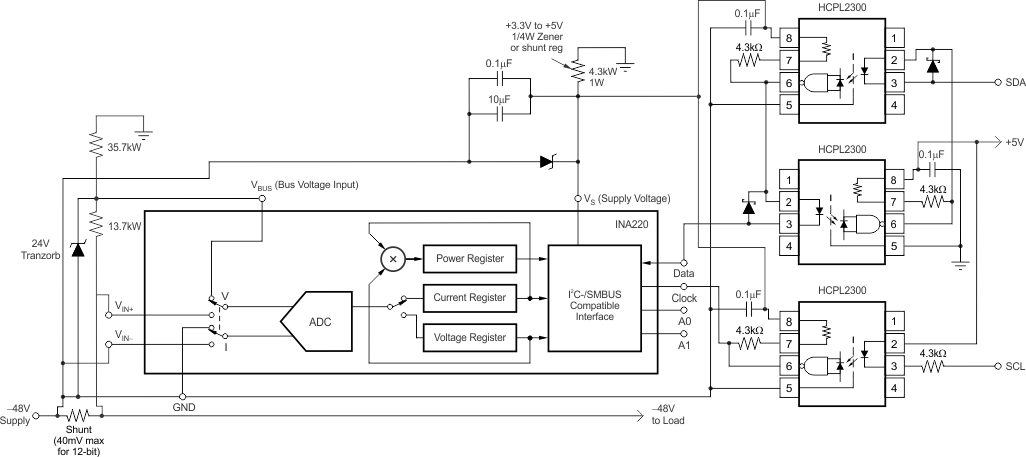 Figure 31. –48-V Telecom Current/Voltage/Power Sense With Isolation
9.2.4 Typical Application: 48-V Telecom Current/Voltage/Power Sense
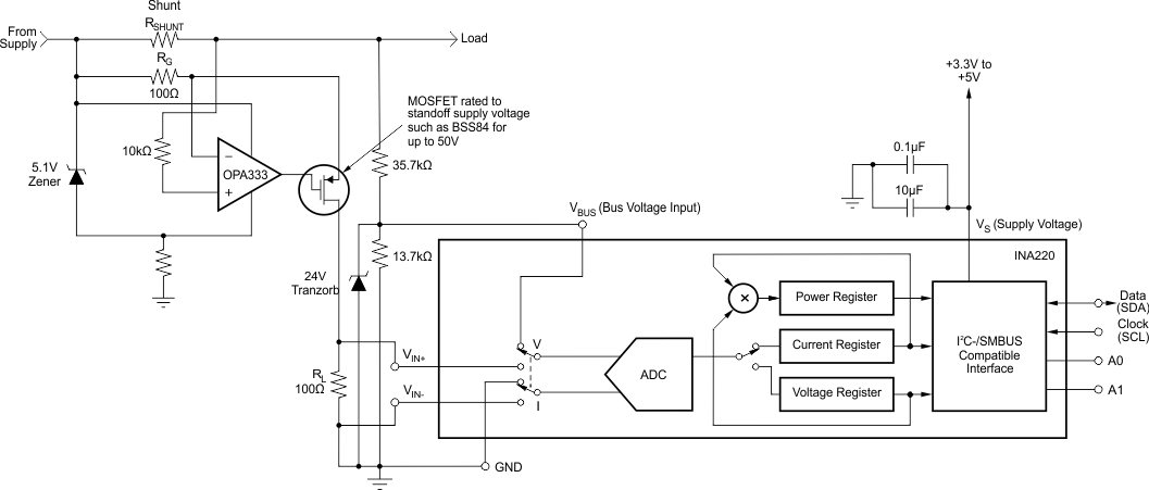 Figure 32. 48-V Telecom Current/Voltage/Power Sense
9.2.5 Typical Application: General Source Low-Side Sensing
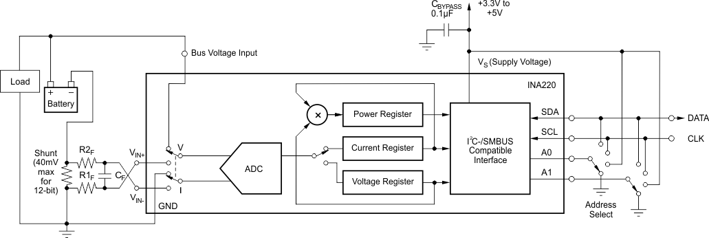 Figure 33. General Source Low-Side Sensing