SBOS612A February 2014 – March 2014 INA225
PRODUCTION DATA.
- 1 Features
- 2 Applications
- 3 Description
- 4 Revision History
- 5 Terminal Configuration and Functions
- 6 Specifications
- 7 Detailed Description
- 8 Applications and Implementation
- 9 Power Supply Recommendations
- 10Layout
- 11Device and Documentation Support
- 12Mechanical, Packaging, and Orderable Information
Package Options
Mechanical Data (Package|Pins)
- DGK|8
Thermal pad, mechanical data (Package|Pins)
Orderable Information
1 Features
- Wide Common-Mode Range: 0 V to 36 V
- Offset Voltage: ±150 μV (Max, All Gains)
- Offset Voltage Drift: 0.5 μV/°C (Max)
- Gain Accuracy, Over Temperature (Max):
- 25 V/V, 50 V/V: ±0.15%
- 100 V/V: ±0.2%
- 200 V/V: ±0.3%
- 10-ppm/°C Gain Drift
- 250-kHz Bandwidth (Gain = 25 V/V)
- Programmable Gains:
- G1 = 25 V/V
- G2 = 50 V/V
- G3 = 100 V/V
- G4 = 200 V/V
- Quiescent Current: 350 μA (Max)
- Package: MSOP-8
2 Applications
- Power Supplies
- Motor Control
- Computers
- Telecom Equipment
- Power Management
- Test and Measurement
3 Description
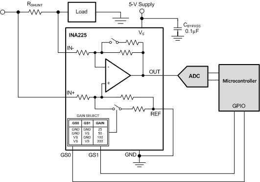
The INA225 is a voltage-output, current-sense amplifier that senses drops across current-sensing resistors at common-mode voltages that can vary from 0 V to 36 V, independent of the supply voltage. The device is a bidirectional, current-shunt monitor that allows an external reference to be used to measure current flowing in both directions across a current-sensing resistor.
Four discrete gain levels are selectable using the two gain-select terminals (GS0 and GS1) to program gains of 25 V/V, 50 V/V, 100 V/V, and 200 V/V. The low-offset, zero-drift architecture and precision gain values enable current-sensing with maximum drops across the shunt as low as 10 mV of full-scale while maintaining very high accuracy measurements over the entire operating temperature range.
The device operates from a single +2.7-V to +36-V power supply, drawing a maximum of 350 μA of supply current. The device is specified over the extended operating temperature range (–40°C to +125°C), and is offered in an MSOP-8 package.
Device Information
| ORDER NUMBER | PACKAGE | BODY SIZE |
|---|---|---|
| INA225AIDGK | MSOP (8) | 3,0 mm x 3,0 mm |
