SBOS743B July 2015 – September 2024 INA226-Q1
PRODUCTION DATA
- 1
- 1 Features
- 2 Applications
- 3 Description
- 4 Pin Configuration and Functions
- 5 Specifications
-
6 Detailed Description
- 6.1 Overview
- 6.2 Functional Block Diagram
- 6.3 Feature Description
- 6.4 Device Functional Modes
- 6.5 Programming
-
7 Registers
- 7.1
Register Maps
- 7.1.1 Configuration Register (00h) (Read/Write)
- 7.1.2 Shunt Voltage Register (01h) (Read-Only)
- 7.1.3 Bus Voltage Register (02h) (Read-Only) #GUID-792F23A7-1E45-4FB9-9334-0BF769622DE4/SBOS5477597
- 7.1.4 Power Register (03h) (Read-Only)
- 7.1.5 Current Register (04h) (Read-Only)
- 7.1.6 Calibration Register (05h) (Read/Write)
- 7.1.7 Mask/Enable Register (06h) (Read/Write)
- 7.1.8 Alert Limit Register (07h) (Read/Write)
- 7.1.9 Manufacturer ID Register (FEh) (Read-Only)
- 7.1.10 Die ID Register (FFh) (Read-Only)
- 7.1
Register Maps
- 8 Application and Implementation
- 9 Device and Documentation Support
- 10Revision History
- 11Mechanical, Packaging, and Orderable Information
Package Options
Mechanical Data (Package|Pins)
- DGS|10
Thermal pad, mechanical data (Package|Pins)
Orderable Information
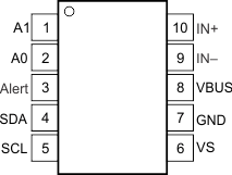
4 Pin Configuration and Functions
 Figure 4-1 DGS Package10-Pin VSSOPTop View
Table 4-1 Pin Functions
| PIN | Type | DESCRIPTION | |
|---|---|---|---|
| NAME | NO. | ||
| A0 | 2 | Digital input | Address pin. Connect to GND, SCL, SDA, or VS. Table 6-2 shows pin settings and corresponding addresses. |
| A1 | 1 | Digital input | Address pin. Connect to GND, SCL, SDA, or VS. Table 6-2 shows pin settings and corresponding addresses. |
| Alert | 3 | Digital output | Multi-functional alert, open-drain output. |
| GND | 7 | Analog | Ground. |
| IN+ | 10 | Analog input | Connect to supply side of shunt resistor. |
| IN– | 9 | Analog input | Connect to load side of shunt resistor. |
| SCL | 5 | Digital input | Serial bus clock line, open-drain input. |
| SDA | 4 | Digital I/O | Serial bus data line, open-drain input/output. |
| VBUS | 8 | Analog input | Bus voltage input. |
| VS | 6 | Analog | Power supply, 2.7 V to 5.5 V. |