SBOS743A July   2015  – May 2020 INA226-Q1

PRODUCTION DATA.  

  1. Features
  2. Applications
  3. Description
    1.     Device Images
      1.      High-Side or Low-Side Sensing Application
  4. Revision History
  5. Pin Configuration and Functions
    1.     Pin Functions
  6. Specifications
    1. 6.1 Absolute Maximum Ratings
    2. 6.2 ESD Ratings
    3. 6.3 Recommended Operating Conditions
    4. 6.4 Thermal Information
    5. 6.5 Electrical Characteristics
    6. 6.6 Typical Characteristics
  7. Detailed Description
    1. 7.1 Overview
    2. 7.2 Functional Block Diagram
    3. 7.3 Feature Description
      1. 7.3.1 Basic ADC Functions
        1. 7.3.1.1 Power Calculation
        2. 7.3.1.2 Alert Pin
    4. 7.4 Device Functional Modes
      1. 7.4.1 Averaging and Conversion Time Considerations
      2. 7.4.2 Filtering and Input Considerations
    5. 7.5 Programming
      1. 7.5.1 Programming the Calibration Register
      2. 7.5.2 Programming the Power Measurement Engine
        1. 7.5.2.1 Calibration Register and Scaling
      3. 7.5.3 Simple Current Shunt Monitor Usage (No Programming Necessary)
      4. 7.5.4 Default Settings
      5. 7.5.5 Bus Overview
        1. 7.5.5.1 Serial Bus Address
        2. 7.5.5.2 Serial Interface
        3. 7.5.5.3 Writing to and Reading from the INA226-Q1
          1. 7.5.5.3.1 High-Speed I2C Mode
        4. 7.5.5.4 SMBus Alert Response
    6. 7.6 Register Maps
      1. Table 4. Register Set Summary
      2. 7.6.1    Configuration Register (00h) (Read/Write)
        1. Table 5. Configuration Register (00h) (Read/Write) Descriptions
      3. 7.6.2    Shunt Voltage Register (01h) (Read-Only)
        1. Table 10. Shunt Voltage Register (01h) (Read-Only) Description
      4. 7.6.3    Bus Voltage Register (02h) (Read-Only)
        1. Table 11. Bus Voltage Register (02h) (Read-Only) Description
      5. 7.6.4    Power Register (03h) (Read-Only)
        1. Table 12. Power Register (03h) (Read-Only) Description
      6. 7.6.5    Current Register (04h) (Read-Only)
        1. Table 13. Current Register (04h) (Read-Only) Register Description
      7. 7.6.6    Calibration Register (05h) (Read/Write)
        1. Table 14. Calibration Register (05h) (Read/Write) Description
      8. 7.6.7    Mask/Enable Register (06h) (Read/Write)
        1. Table 15. Mask/Enable Register (06h) (Read/Write)
      9. 7.6.8    Alert Limit Register (07h) (Read/Write)
        1. Table 16. Alert Limit Register (07h) (Read/Write) Description
      10. 7.6.9    Manufacturer ID Register (FEh) (Read-Only)
        1. Table 17. Manufacturer ID Register (FEh) (Read-Only) Description
      11. 7.6.10   Die ID Register (FFh) (Read-Only)
        1. Table 18. Die ID Register (FFh) (Read-Only) Description
  8. Application and Implementation
    1. 8.1 Application Information
    2. 8.2 Typical Applications
      1. 8.2.1 High-Side Sensing Circuit Application
        1. 8.2.1.1 Design Requirements
        2. 8.2.1.2 Detailed Design Procedure
        3. 8.2.1.3 Application Curves
          1. Table 19. Configuration Register (00h) Settings for (Value = 4025h)
          2. Table 20. Configuration Register (00h) Settings for (Value = 4005h)
          3. Table 21. Mask/Enable Register (06h) Settings for and (Value = 8000h)
          4. Table 22. Alert Limit Register (07h) Settings for and (Value = 7D00)
  9. Power Supply Recommendations
  10. 10Layout
    1. 10.1 Layout Guidelines
    2. 10.2 Layout Example
  11. 11Device and Documentation Support
    1. 11.1 Device Support
      1. 11.1.1 Development Support
    2. 11.2 Support Resources
    3. 11.3 Trademarks
    4. 11.4 Electrostatic Discharge Caution
    5. 11.5 Glossary
  12. 12Mechanical, Packaging, and Orderable Information

Package Options

Mechanical Data (Package|Pins)
Thermal pad, mechanical data (Package|Pins)
Orderable Information

Typical Characteristics

At TA = 25°C, VVS = 3.3 V, VIN+ = 12 V, VSENSE = (VIN+ – VIN–) = 0 mV and VVBUS = 12 V, unless otherwise noted.
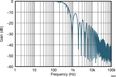
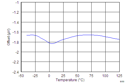
INA226-Q1 g001_bos547.gif
Figure 1. Frequency Response
INA226-Q1 g003_bos547.png
Figure 3. Shunt Input Offset Voltage vs Temperature
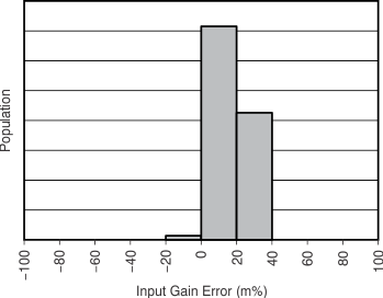
INA226-Q1 tc_histo_shunt_input_gain_err_distrib_bos547.gif
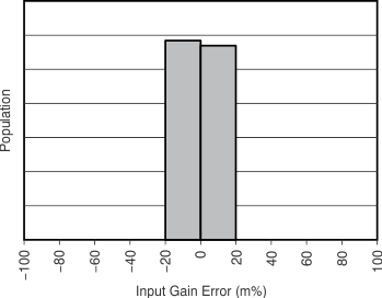
Figure 5. Shunt Input Gain Error Production Distribution
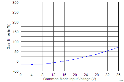
INA226-Q1 g007_bos547.png
Figure 7. Shunt Input Gain Error vs Common-Mode Voltage
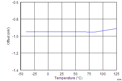
INA226-Q1 g010_bos547.png
Figure 9. Bus Input Offset Voltage vs Temperature
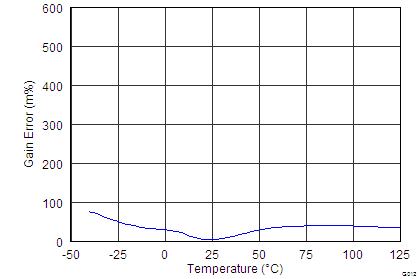
INA226-Q1 g013_bos547.png
Figure 11. Bus Input Gain Error vs Temperature
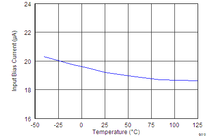
INA226-Q1 g016_bos547.png
Figure 13. Input Bias Current vs Temperature
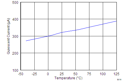
INA226-Q1 g018_bos547.png
Figure 15. Active IQ vs Temperature
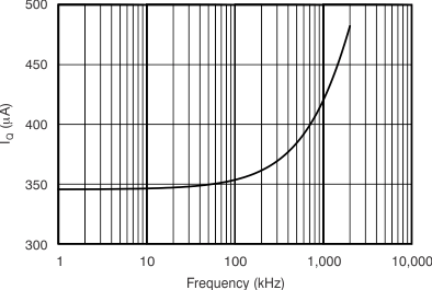
INA226-Q1 tc_active_iq_fqcy_bos547.gif
Figure 17. Active IQ vs I2C Clock Frequency
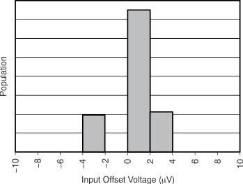
INA226-Q1 tc_histo_shunt_input_offset_v_distrib_bos547.gif
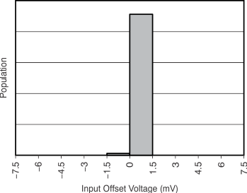
Figure 2. Shunt Input Offset Voltage Production Distribution
INA226-Q1 g004_bos547.png
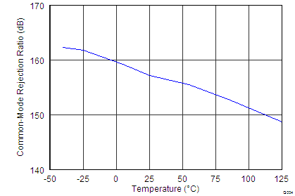
Figure 4. Shunt Input Common-Mode Rejection Ratio vs Temperature
INA226-Q1 g006_new_bos547.png
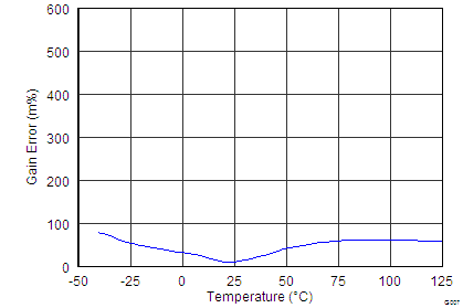
Figure 6. Shunt Input Gain Error vs Temperature
INA226-Q1 tc_histo_bus_input_offset_v_distrib_bos547.gif
Figure 8. Bus Input Offset Voltage Production Distribution
INA226-Q1 tc_histo_bus_input_gain_err_distrib_bos547.gif
Figure 10. Bus Input Gain Error Production Distribution
INA226-Q1 g015_bos547.png
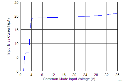
Figure 12. Input Bias Current vs Common-Mode Voltage
INA226-Q1 g017_bos547.png
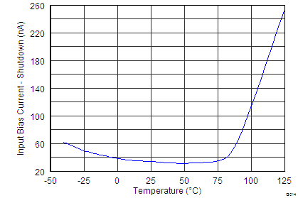
Figure 14. Input Bias Current vs Temperature, Shutdown
INA226-Q1 g019_bos547.png
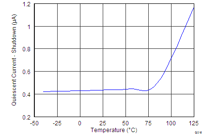
Figure 16. Shutdown IQ vs Temperature
INA226-Q1 tc_shutdown_iq_i2c_fqcy_bos547.gif
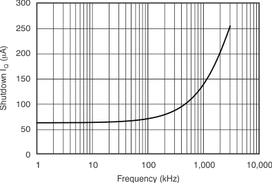
Figure 18. Shutdown IQ vs I2C Clock Frequency