SBOS644D February 2013 – July 2022 INA231
PRODUCTION DATA
- 1 Features
- 2 Applications
- 3 Description
- 4 Revision History
- 5 Device Comparison
- 6 Pin Configuration and Functions
- 7 Specifications
-
8 Detailed Description
- 8.1 Overview
- 8.2 Functional Block Diagram
- 8.3 Feature Description
- 8.4 Device Functional Modes
- 8.5 Programming
- 8.6
Register Maps
- 8.6.1 Configuration Register (00h, Read/Write)
- 8.6.2 Shunt Voltage Register (01h, Read-Only)
- 8.6.3 Bus Voltage Register (02h, Read-Only)
- 8.6.4 Power Register (03h, Read-Only)
- 8.6.5 Current Register (04h, Read-Only)
- 8.6.6 Calibration Register (05h, Read/Write)
- 8.6.7 Mask/Enable Register (06h, Read/Write)
- 8.6.8 Alert Limit Register (07h, Read/Write)
- 9 Application and Implementation
- 10Device and Documentation Support
- 11Mechanical, Packaging, and Orderable Information
Package Options
Refer to the PDF data sheet for device specific package drawings
Mechanical Data (Package|Pins)
- YFF|12
- YFD|12
Thermal pad, mechanical data (Package|Pins)
Orderable Information
9.1.1 Filtering and Input Considerations
Measuring current is often a noisy task, and such noise can be difficult to define. The INA231 offers several options for filtering by allowing the conversion times and number of averages to be independently selected in the Configuration register. The conversion times can be independently set for the shunt voltage and bus voltage measurements to allow added flexibility in configuring the monitoring of the power-supply bus.
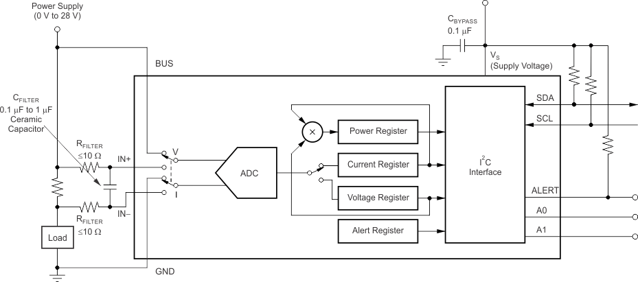
The internal ADC is based on a delta-sigma (ΔΣ) front-end with a 500-kHz (±30%) typical sampling rate. This architecture has good inherent noise rejection; however, transients that occur at or very close to the sampling rate harmonics can cause problems. These signals are at 1 MHz and higher; therefore, manage them by incorporating filtering at the input of the INA231. The high frequency enables the use of low-value series resistors on the filter with negligible effects on measurement accuracy. In general, filtering the INA231 input is only necessary if there are transients at exact harmonics of the 500-kHz (±30%) sampling rate (greater than 1 MHz). Filter using the lowest possible series resistance (typically 10 Ω or less) and a ceramic capacitor. Recommended values for this capacitor are 0.1 μF to 1.0 μF. Figure 9-2 shows the INA231 with an additional filter added at the input.
 Figure 9-2 INA231 With Input Filtering
Overload conditions are another consideration for the INA231 inputs. The INA231 inputs are specified to tolerate 30 V across the inputs. A large differential scenario might be a short to ground on the load side of the shunt. This type of event can result in full power-supply voltage across the shunt (as long as the power supply or energy storage capacitors support it). Keep in mind that removing a short to ground can result in inductive kickbacks that could exceed the 30-V differential and common-mode rating of the INA231. Inductive kickback voltages are best controlled by zener-type transient-absorbing devices (commonly called transzorbs) combined with sufficient energy storage capacitance.
In applications that do not have large energy-storage electrolytics on one or both sides of the shunt, an input overstress condition may result from an excessive dV/dt of the voltage applied to the input. A hard physical short is the most likely cause of this event, particularly in applications with no large electrolytics present. This problem occurs because an excessive dV/dt can activate the ESD protection in the INA231 in systems where large currents are available. Testing has demonstrated that the addition of 10-Ω resistors in series with each input of the INA231 sufficiently protect the inputs against this dV/dt failure up to the 30-V rating of the INA231. Selecting these resistors in the range noted has minimal effect on accuracy.