SBOSA20A February 2021 – May 2022 INA237
PRODUCTION DATA
- 1 Features
- 2 Applications
- 3 Description
- 4 Revision History
- 5 Pin Configuration and Functions
- 6 Specifications
-
7 Detailed Description
- 7.1 Overview
- 7.2 Functional Block Diagram
- 7.3 Feature Description
- 7.4 Device Functional Modes
- 7.5 Programming
- 7.6 Register Maps
- 8 Application and Implementation
- 9 Power Supply Recommendations
- 10Layout
- 11Device and Documentation Support
- 12Mechanical, Packaging, and Orderable Information
Package Options
Mechanical Data (Package|Pins)
- DGS|10
Thermal pad, mechanical data (Package|Pins)
Orderable Information
8.2.3 Application Curves
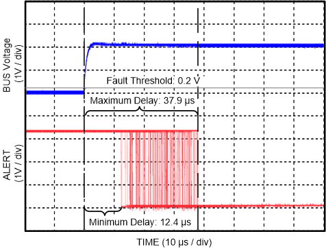
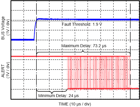
Figure 8-3 and Figure 8-4 show the ALERT pin response to a bus overvoltage fault with a conversion time of 50 μs, averaging set to 1, and the SLOWALERT bit set to 0 for bus only conversions. For these scope shots, persistence was enabled on the ALERT channel to show the variation in the alert response for many sequential fault events. If the magnitude of the fault is sufficient the ALERT response can be as fast as one quarter of the ADC conversion time as shown in Figure 8-3. For fault conditions that are just exceeding the limit threshold, the response time for the ALERT pin can vary from approximately 0.5 to 1.5 conversion cycles as shown in Figure 8-4. Variation in the alert response exists because the external fault event is not synchronized to the internal ADC conversion start. Also the ADC is constantly sampling to get a result, so the response time for fault events starting from zero will slower than fault events starting from values near the set fault threshold. Since the timing of the alert can be difficult to predict, applications where the alert timing is critical should assume a alert response equal to 1.5 times the ADC conversion time for bus voltage or shunt voltage only conversions.
 Figure 8-3 Alert Response Time
(Sampled Values Significantly Above Threshold)
 Figure 8-4 Alert Response Time
(Sampled Values Slightly Above Threshold)