SLYS026A June   2020  – June 2021 INA238-Q1

PRODUCTION DATA  

  1. Features
  2. Applications
  3. Description
  4. Revision History
  5. Pin Configuration and Functions
  6. Specifications
    1. 6.1 Absolute Maximum Ratings
    2. 6.2 ESD Ratings
    3. 6.3 Recommended Operating Conditions
    4. 6.4 Thermal Information
    5. 6.5 Electrical Characteristics
    6. 6.6 Timing Requirements (I2C)
    7. 6.7 Timing Diagram
    8. 6.8 Typical Characteristics
  7. Detailed Description
    1. 7.1 Overview
    2. 7.2 Functional Block Diagram
    3. 7.3 Feature Description
      1. 7.3.1 Versatile High Voltage Measurement Capability
      2. 7.3.2 Power Calculation
      3. 7.3.3 Low Bias Current
      4. 7.3.4 High-Precision Delta-Sigma ADC
        1. 7.3.4.1 Low Latency Digital Filter
        2. 7.3.4.2 Flexible Conversion Times and Averaging
      5. 7.3.5 Integrated Precision Oscillator
      6. 7.3.6 Multi-Alert Monitoring and Fault Detection
    4. 7.4 Device Functional Modes
      1. 7.4.1 Shutdown Mode
      2. 7.4.2 Power-On Reset
    5. 7.5 Programming
      1. 7.5.1 I2C Serial Interface
        1. 7.5.1.1 Writing to and Reading Through the I2C Serial Interface
        2. 7.5.1.2 High-Speed I2C Mode
        3. 7.5.1.3 SMBus Alert Response
    6. 7.6 Register Maps
      1. 7.6.1 INA238-Q1 Registers
  8. Application and Implementation
    1. 8.1 Application Information
      1. 8.1.1 Device Measurement Range and Resolution
      2. 8.1.2 Current and Power Calculations
      3. 8.1.3 ADC Output Data Rate and Noise Performance
      4. 8.1.4 Input Filtering Considerations
    2. 8.2 Typical Application
      1. 8.2.1 Design Requirements
      2. 8.2.2 Detailed Design Procedure
        1. 8.2.2.1 Select the Shunt Resistor
        2. 8.2.2.2 Configure the Device
        3. 8.2.2.3 Program the Shunt Calibration Register
        4. 8.2.2.4 Set Desired Fault Thresholds
        5. 8.2.2.5 Calculate Returned Values
      3. 8.2.3 Application Curves
  9. Power Supply Recommendations
  10. 10Layout
    1. 10.1 Layout Guidelines
    2. 10.2 Layout Example
  11. 11Device and Documentation Support
    1. 11.1 Receiving Notification of Documentation Updates
    2. 11.2 Support Resources
    3. 11.3 Trademarks
    4. 11.4 Electrostatic Discharge Caution
    5. 11.5 Glossary
  12. 12Mechanical, Packaging, and Orderable Information

Package Options

Mechanical Data (Package|Pins)
Thermal pad, mechanical data (Package|Pins)
Orderable Information

Low Latency Digital Filter

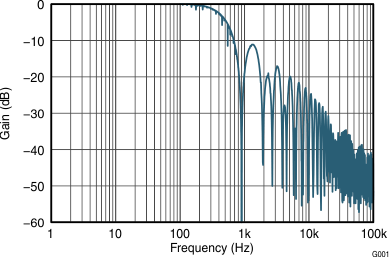
The device integrates a low-pass digital filter that performs both decimation and filtering on the ADC output data, which helps with noise reduction. The digital filter is automatically adjusted for the different output data rates and always settles within one conversion cycle. The user has the flexibility to choose different output conversion time periods TCT from 50 µs to 4.12 ms. With this configuration the first amplitude notch appears at the Nyquist frequency of the output signal which is determined by the selected conversion time period and defined as fNOTCH= 1 / (2 x TCT). This means that the filter cut-off frequency will scale proportionally with the data output rate as described. Figure 7-3 shows the filter response when the 1.052 ms conversion time period is selected.
GUID-1EAF593E-D243-4AB9-AB67-F955CBA8189D-low.gif
Conversion time = 1.052 ms, single conversion only
Figure 7-3 ADC Frequency Response