SLYS026A June 2020 – June 2021 INA238-Q1
PRODUCTION DATA
- 1 Features
- 2 Applications
- 3 Description
- 4 Revision History
- 5 Pin Configuration and Functions
- 6 Specifications
-
7 Detailed Description
- 7.1 Overview
- 7.2 Functional Block Diagram
- 7.3 Feature Description
- 7.4 Device Functional Modes
- 7.5 Programming
- 7.6 Register Maps
- 8 Application and Implementation
- 9 Power Supply Recommendations
- 10Layout
- 11Device and Documentation Support
- 12Mechanical, Packaging, and Orderable Information
Package Options
Mechanical Data (Package|Pins)
- DGS|10
Thermal pad, mechanical data (Package|Pins)
Orderable Information
3 Description
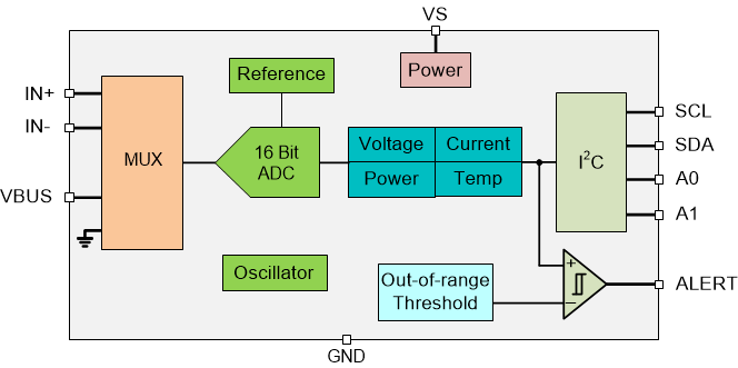
The INA238-Q1 is an ultra-precise digital power monitor with a 16-bit delta-sigma ADC specifically designed for current-sensing applications. The device can measure a full-scale differential input of ±163.84 mV or ±40.96 mV across a resistive shunt sense element with common-mode voltage support from –0.3 V to +85 V.
The INA238-Q1 reports current, bus voltage, temperature, and power, all while performing the needed calculations in the background. The integrated temperature sensor is ±1°C accurate for die temperature measurement and is useful in monitoring the system ambient temperature.
The low offset and gain drift design of the INA238-Q1 allows the device to be used in precise systems that do not undergo multi-temperature calibration during manufacturing. Further, the very low offset voltage and noise allow for use in A to kA sensing applications and provide a wide dynamic range without significant power dissipation losses on the sensing shunt element. The low input bias current of the device permits the use of larger current-sense resistors, thus providing accurate current measurements in the micro-amp range.
The device allows for selectable ADC conversion times from 50 µs to 4.12 ms as well as sample averaging from 1x to 1024x, which further helps reduce the noise of the measured data.
| PART NUMBER | PACKAGE | BODY SIZE (NOM) |
|---|---|---|
| INA238-Q1 | VSSOP (10) | 3.00 mm × 3.00 mm |
 Simplified Block
Diagram