SLYS026A June   2020  – June 2021 INA238-Q1

PRODUCTION DATA  

  1. Features
  2. Applications
  3. Description
  4. Revision History
  5. Pin Configuration and Functions
  6. Specifications
    1. 6.1 Absolute Maximum Ratings
    2. 6.2 ESD Ratings
    3. 6.3 Recommended Operating Conditions
    4. 6.4 Thermal Information
    5. 6.5 Electrical Characteristics
    6. 6.6 Timing Requirements (I2C)
    7. 6.7 Timing Diagram
    8. 6.8 Typical Characteristics
  7. Detailed Description
    1. 7.1 Overview
    2. 7.2 Functional Block Diagram
    3. 7.3 Feature Description
      1. 7.3.1 Versatile High Voltage Measurement Capability
      2. 7.3.2 Power Calculation
      3. 7.3.3 Low Bias Current
      4. 7.3.4 High-Precision Delta-Sigma ADC
        1. 7.3.4.1 Low Latency Digital Filter
        2. 7.3.4.2 Flexible Conversion Times and Averaging
      5. 7.3.5 Integrated Precision Oscillator
      6. 7.3.6 Multi-Alert Monitoring and Fault Detection
    4. 7.4 Device Functional Modes
      1. 7.4.1 Shutdown Mode
      2. 7.4.2 Power-On Reset
    5. 7.5 Programming
      1. 7.5.1 I2C Serial Interface
        1. 7.5.1.1 Writing to and Reading Through the I2C Serial Interface
        2. 7.5.1.2 High-Speed I2C Mode
        3. 7.5.1.3 SMBus Alert Response
    6. 7.6 Register Maps
      1. 7.6.1 INA238-Q1 Registers
  8. Application and Implementation
    1. 8.1 Application Information
      1. 8.1.1 Device Measurement Range and Resolution
      2. 8.1.2 Current and Power Calculations
      3. 8.1.3 ADC Output Data Rate and Noise Performance
      4. 8.1.4 Input Filtering Considerations
    2. 8.2 Typical Application
      1. 8.2.1 Design Requirements
      2. 8.2.2 Detailed Design Procedure
        1. 8.2.2.1 Select the Shunt Resistor
        2. 8.2.2.2 Configure the Device
        3. 8.2.2.3 Program the Shunt Calibration Register
        4. 8.2.2.4 Set Desired Fault Thresholds
        5. 8.2.2.5 Calculate Returned Values
      3. 8.2.3 Application Curves
  9. Power Supply Recommendations
  10. 10Layout
    1. 10.1 Layout Guidelines
    2. 10.2 Layout Example
  11. 11Device and Documentation Support
    1. 11.1 Receiving Notification of Documentation Updates
    2. 11.2 Support Resources
    3. 11.3 Trademarks
    4. 11.4 Electrostatic Discharge Caution
    5. 11.5 Glossary
  12. 12Mechanical, Packaging, and Orderable Information

Package Options

Mechanical Data (Package|Pins)
Thermal pad, mechanical data (Package|Pins)
Orderable Information

Typical Application

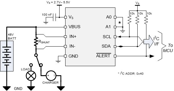
The low offset voltage and low input bias current of the INA238-Q1 allow accurate monitoring of a wide range of currents. To accurately monitor currents with high resolution, select the value of the shunt resistor so that the resulting sense voltage is close to the maximum allowable differential input voltage range (either ±163.84 mV or ±40.96 mV, depending on register settings). The circuit for monitoring currents in a high-side configuration is shown in Figure 8-2.
GUID-070EB83A-B940-4E77-B7B3-86798D3231EC-low.gif Figure 8-2 INA238-Q1 High-Side Sensing Application Diagram