SLYS026A
June 2020 – June 2021
INA238-Q1
PRODUCTION DATA
1
Features
2
Applications
3
Description
4
Revision History
5
Pin Configuration and Functions
6
Specifications
6.1
Absolute Maximum Ratings
6.2
ESD Ratings
6.3
Recommended Operating Conditions
6.4
Thermal Information
6.5
Electrical Characteristics
6.6
Timing Requirements (I2C)
6.7
Timing Diagram
6.8
Typical Characteristics
7
Detailed Description
7.1
Overview
7.2
Functional Block Diagram
7.3
Feature Description
7.3.1
Versatile High Voltage Measurement Capability
7.3.2
Power Calculation
7.3.3
Low Bias Current
7.3.4
High-Precision Delta-Sigma ADC
7.3.4.1
Low Latency Digital Filter
7.3.4.2
Flexible Conversion Times and Averaging
7.3.5
Integrated Precision Oscillator
7.3.6
Multi-Alert Monitoring and Fault Detection
7.4
Device Functional Modes
7.4.1
Shutdown Mode
7.4.2
Power-On Reset
7.5
Programming
7.5.1
I2C Serial Interface
7.5.1.1
Writing to and Reading Through the I2C Serial Interface
7.5.1.2
High-Speed I2C Mode
7.5.1.3
SMBus Alert Response
7.6
Register Maps
7.6.1
INA238-Q1 Registers
8
Application and Implementation
8.1
Application Information
8.1.1
Device Measurement Range and Resolution
8.1.2
Current and Power Calculations
8.1.3
ADC Output Data Rate and Noise Performance
8.1.4
Input Filtering Considerations
8.2
Typical Application
8.2.1
Design Requirements
8.2.2
Detailed Design Procedure
8.2.2.1
Select the Shunt Resistor
8.2.2.2
Configure the Device
8.2.2.3
Program the Shunt Calibration Register
8.2.2.4
Set Desired Fault Thresholds
8.2.2.5
Calculate Returned Values
8.2.3
Application Curves
9
Power Supply Recommendations
10
Layout
10.1
Layout Guidelines
10.2
Layout Example
11
Device and Documentation Support
11.1
Receiving Notification of Documentation Updates
11.2
Support Resources
11.3
Trademarks
11.4
Electrostatic Discharge Caution
11.5
Glossary
12
Mechanical, Packaging, and Orderable Information
Package Options
Mechanical Data (Package|Pins)
DGS|10
MPDS035C
Thermal pad, mechanical data (Package|Pins)
Orderable Information
slys026a_oa
slys026a_pm
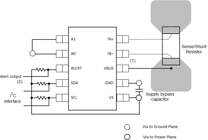
10.2
Layout Example
(1) Connect the VBUS pin to the voltage powering the load for load power calculations..
(2) Can be left floating if unused.
Figure 10-1
INA238-Q1
Layout Example