SBOS950A July 2019 – January 2021 INA253-Q1
PRODUCTION DATA
- 1 Features
- 2 Applications
- 3 Description
- 4 Revision History
- 5 Pin Configuration and Functions
- 6 Specifications
-
7 Detailed Description
- 7.1 Overview
- 7.2 Functional Block Diagram
- 7.3 Feature Description
- 7.4
Device Functional Modes
- 7.4.1 Adjusting the Output Midpoint With the Reference Pins
- 7.4.2 Reference Pin Connections for Unidirectional Current Measurements
- 7.4.3 Ground Referenced Output
- 7.4.4 Reference Pin Connections for Bidirectional Current Measurements
- 7.4.5 Output Set to Mid-Supply Voltage
- 7.4.6 Output Set to Mid-External Reference
- 7.4.7 Output Set Using Resistor Divide
- 8 Application and Implementation
- 9 Power Supply Recommendations
- 10Layout
- 11Device and Documentation Support
- 12Mechanical, Packaging, and Orderable Information
Package Options
Mechanical Data (Package|Pins)
- PW|20
Thermal pad, mechanical data (Package|Pins)
Orderable Information
3 Description
The INA253-Q1 is an automotive, voltage-output, current sense amplifier with an integrated shunt resistor of 2 mΩ. The INA253-Q1 monitors bidirectional currents over a wide common-mode range from –4 V to +80 V, independent of the supply voltage. Three fixed gains are available: 100 mV/A, 200 mV/A, and 400 mV/A. The integration of the precision resistor with a zero-drift chopped amplifier provides calibration-equivalent measurement accuracy, ultra-low temperature-drift performance of 15 ppm/ °C, and an optimized Kelvin layout for the sensing resistor.
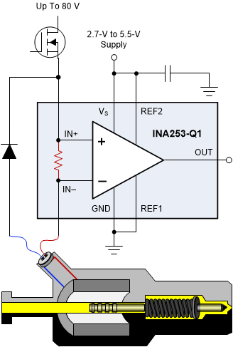
The INA253-Q1 is designed with enhanced PWM rejection circuitry to suppress large (dv/dt) signals that enable real-time continuous current measurements. The measurements are critical for in-line current measurements in a motor-drive application, and for solenoid valve-control applications.
This device operates from a single 2.7-V to 5.5-V power supply, drawing a maximum of 3 mA of supply current. All gain versions are specified over the operating temperature range of –40 °C to +125 °C, and are available in a 20-pin TSSOP package.
| PART NUMBER | PACKAGE | BODY SIZE (NOM) |
|---|---|---|
| INA253-Q1 | TSSOP (20) | 6.50 mm × 4.40 mm |
 Typical Application