SBOS401C July 2007 – April 2016 INA270A-Q1 , INA271A-Q1
PRODUCTION DATA.
- 1 Features
- 2 Applications
- 3 Description
- 4 Revision History
- 5 Device Comparison Table
- 6 Pin Configuration and Functions
- 7 Specifications
- 8 Detailed Description
- 9 Application and Implementation
- 10Power Supply Recommendations
- 11Layout
- 12Device and Documentation Support
- 13Mechanical, Packaging, and Orderable Information
Package Options
Mechanical Data (Package|Pins)
- D|8
Thermal pad, mechanical data (Package|Pins)
Orderable Information
10 Power Supply Recommendations
The input circuitry of the INA27xA-Q1 can accurately measure beyond its power-supply voltage, VS. For example, the VS power supply can be 5 V, whereas the load power-supply voltage is up to 80 V. The output voltage range of the OUT terminal, however, is limited by the voltages on the power-supply pin.
10.1 Shutdown
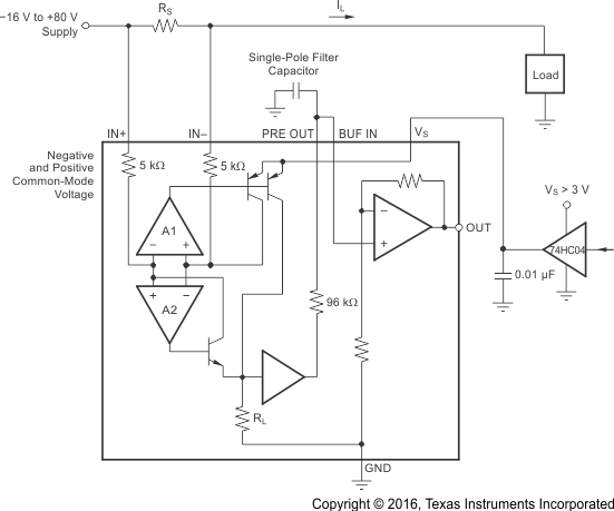
The INA27xA-Q1 devices do not provide a shutdown pin; however, because they consume a quiescent current less than 1 mA, they can be powered by either the output of logic gates or by transistor switches to supply power. Driving the gate low shuts down the INA27xA-Q1. Use a totem-pole output buffer or gate that can provide sufficient drive along with 0.1-μF bypass capacitor, preferably ceramic with good high-frequency characteristics. This gate should have a supply voltage of 3 V or greater, because the INA27xA-Q1 requires a minimum supply greater than 2.7 V. In addition to eliminating quiescent current, this gate also turns off the 10-μA bias current present at each of the inputs.
NOTE
The IN+ and IN– inputs are able to withstand full common-mode voltage under all powered and under-powered conditions. Figure 22 shows an example of the shutdown circuit.
 Figure 22. INA27xA-Q1 Example Shutdown Circuit Schematic