SBOSA32C February   2023  – December 2024 INA296A-Q1 , INA296B-Q1

PRODUCTION DATA  

  1.   1
  2. Features
  3. Applications
  4. Description
  5. Device Comparison
  6. Pin Configuration and Functions
  7. Specifications
    1. 6.1 Absolute Maximum Ratings
    2. 6.2 ESD Ratings
    3. 6.3 Recommended Operating Conditions
    4. 6.4 Thermal Information
    5. 6.5 Electrical Characteristics
    6. 6.6 Typical Characteristics
  8. Detailed Description
    1. 7.1 Overview
    2. 7.2 Functional Block Diagram
    3. 7.3 Feature Description
      1. 7.3.1 Amplifier Input Common-Mode Signal
        1. 7.3.1.1 Input-Signal Bandwidth
        2. 7.3.1.2 Low Input Bias Current
        3. 7.3.1.3 Low VSENSE Operation
        4. 7.3.1.4 Wide Fixed Gain Output
        5. 7.3.1.5 Wide Supply Range
    4. 7.4 Device Functional Modes
      1. 7.4.1 Adjusting the Output With the Reference Pins
      2. 7.4.2 Reference Pin Connections for Unidirectional Current Measurements
        1. 7.4.2.1 Ground Referenced Output
        2. 7.4.2.2 VS Referenced Output
      3. 7.4.3 Reference Pin Connections for Bidirectional Current Measurements
        1. 7.4.3.1 Output Set to External Reference Voltage
        2. 7.4.3.2 Output Set to Mid-Supply Voltage
        3. 7.4.3.3 Output Set to Mid-External Reference
        4. 7.4.3.4 Output Set Using Resistor Divider
      4. 7.4.4 High Signal Throughput
  9. Application and Implementation
    1. 8.1 Application Information
      1. 8.1.1 RSENSE and Device Gain Selection
    2. 8.2 Typical Application
      1. 8.2.1 Current Sensing in a Solenoid Application
        1. 8.2.1.1 Design Requirements
        2. 8.2.1.2 Detailed Design Procedure
        3. 8.2.1.3 Application Curve
    3. 8.3 Power Supply Recommendations
      1. 8.3.1 Power Supply Decoupling
    4. 8.4 Layout
      1. 8.4.1 Layout Guidelines
      2. 8.4.2 Layout Examples
  10. Device and Documentation Support
    1. 9.1 Documentation Support
      1. 9.1.1 Related Documentation
    2. 9.2 Receiving Notification of Documentation Updates
    3. 9.3 Support Resources
    4. 9.4 Trademarks
    5. 9.5 Electrostatic Discharge Caution
    6. 9.6 Glossary
  11. 10Revision History
  12. 11Mechanical, Packaging, and Orderable Information

Package Options

Mechanical Data (Package|Pins)
Thermal pad, mechanical data (Package|Pins)
Orderable Information

Output Set Using Resistor Divider

The INA296x-Q1 reference pins allow for the mid-point of the output voltage to be adjusted for system circuitry connections to analog to digital converters (ADCs) or other amplifiers. The reference pins are designed to be connected directly to supply, ground, or a low-impedance reference voltage. The reference pins can be connected together and biased using a resistor divider to achieve a custom output voltage. If the amplifier is used in this configuration, as shown in Figure 7-7, use the output as a differential signal with respect to the resistor divider voltage. Use of the amplifier output as a single-ended signal in this configuration is not recommended because the internal impedance shifts can adversely affect device performance specifications. If single-ended measurement is required, TI recommends to use an external op amp to buffer the resistor divider voltage (see Figure 7-8).
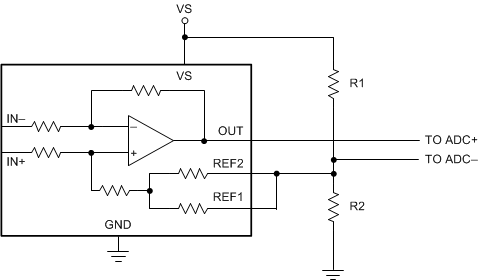
INA296A-Q1 INA296B-Q1 Setting the Reference Using a
                    Resistor Divider Figure 7-7 Setting the Reference Using a Resistor Divider
INA296A-Q1 INA296B-Q1 Setting the Reference Using a
                    Resistor Divider and an Op Amp Buffer Figure 7-8 Setting the Reference Using a Resistor Divider and an Op Amp Buffer