SBOSA32B February   2023  – March 2024 INA296A-Q1 , INA296B-Q1

PRODUCTION DATA  

  1.   1
  2. Features
  3. Applications
  4. Description
  5. Device Comparison
  6. Pin Configuration and Functions
  7. Specifications
    1. 6.1 Absolute Maximum Ratings
    2. 6.2 ESD Ratings
    3. 6.3 Recommended Operating Conditions
    4. 6.4 Thermal Information
    5. 6.5 Electrical Characteristics
    6. 6.6 Typical Characteristics
  8. Detailed Description
    1. 7.1 Overview
    2. 7.2 Functional Block Diagram
    3. 7.3 Feature Description
      1. 7.3.1 Amplifier Input Common-Mode Signal
        1. 7.3.1.1 Input-Signal Bandwidth
        2. 7.3.1.2 Low Input Bias Current
        3. 7.3.1.3 Low VSENSE Operation
        4. 7.3.1.4 Wide Fixed Gain Output
        5. 7.3.1.5 Wide Supply Range
    4. 7.4 Device Functional Modes
      1. 7.4.1 Adjusting the Output With the Reference Pins
      2. 7.4.2 Reference Pin Connections for Unidirectional Current Measurements
        1. 7.4.2.1 Ground Referenced Output
        2. 7.4.2.2 VS Referenced Output
      3. 7.4.3 Reference Pin Connections for Bidirectional Current Measurements
        1. 7.4.3.1 Output Set to External Reference Voltage
        2. 7.4.3.2 Output Set to Mid-Supply Voltage
        3. 7.4.3.3 Output Set to Mid-External Reference
        4. 7.4.3.4 Output Set Using Resistor Divider
      4. 7.4.4 High Signal Throughput
  9. Application and Implementation
    1. 8.1 Application Information
      1. 8.1.1 RSENSE and Device Gain Selection
    2. 8.2 Typical Application
      1. 8.2.1 Current Sensing in a Solenoid Application
        1. 8.2.1.1 Design Requirements
        2. 8.2.1.2 Detailed Design Procedure
        3. 8.2.1.3 Application Curve
    3. 8.3 Power Supply Recommendations
      1. 8.3.1 Power Supply Decoupling
    4. 8.4 Layout
      1. 8.4.1 Layout Guidelines
      2. 8.4.2 Layout Examples
  10. Device and Documentation Support
    1. 9.1 Documentation Support
      1. 9.1.1 Related Documentation
    2. 9.2 Receiving Notification of Documentation Updates
    3. 9.3 Support Resources
    4. 9.4 Trademarks
    5. 9.5 Electrostatic Discharge Caution
    6. 9.6 Glossary
  11. 10Revision History
  12. 11Mechanical, Packaging, and Orderable Information

Package Options

Mechanical Data (Package|Pins)
Thermal pad, mechanical data (Package|Pins)
Orderable Information

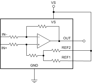
VS Referenced Output

Unidirectional mode with a VS referenced output is configured by connecting both reference pins to the positive supply. Use this configuration for circuits that require power up and stabilization of the amplifier output signal and other control circuitry before power is applied to the load (see Figure 7-3).
GUID-ED2765E5-7D23-4E0E-B132-2B2EFFEC9A7A-low.gifFigure 7-3 VS Referenced Output