SBOS764B December 2015 – December 2021 INA300-Q1
PRODUCTION DATA
- 1 Features
- 2 Applications
- 3 Description
- 4 Revision History
- 5 Pin Configuration and Functions
- 6 Specifications
-
7 Detailed Description
- 7.1 Overview
- 7.2 Functional Block Diagram
- 7.3 Feature Description
- 7.4 Device Functional Modes
- 8 Application and Implementation
- 9 Power Supply Recommendations
- 10Layout
- 11Device and Documentation Support
- 12Mechanical, Packaging, and Orderable Information
Package Options
Mechanical Data (Package|Pins)
- DGS|10
Thermal pad, mechanical data (Package|Pins)
Orderable Information
3 Description
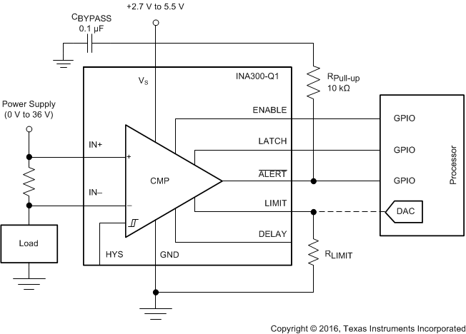
The INA300-Q1 is a high common-mode, current-sensing comparator that detects overcurrent conditions by measuring the voltage developed across a current-sensing or shunt resistor. The device measures this differential voltage signal on common-mode voltages that can vary from 0 V up to 36 V, independent of the supply voltage. The INA300-Q1 device features an adjustable threshold range that is set using a single external limit-setting resistor. A selectable hysteresis feature enables adjustable operation of the comparator to accommodate the wide input signal range of 0 mV to 250 mV.
An open-drain alert output on the device can be configured to operate in either a transparent mode where the output status follows the input state, or in a latched mode where the alert output is cleared when the latch is cleared. The device response time setting is selectable, which enables overcurrent alerts to be issued in as fast as 10 µs.
The INA300-Q1 device operates from a single 2.7-V to 5.5-V supply, drawing a maximum supply current of 135 µA. The INA300-Q1 device is specified over the extended operating temperature range of –40°C to +125°C, and is available in a VSSOP-10 package.
| PART NUMBER | PACKAGE(1) | BODY SIZE (NOM) |
|---|---|---|
| INA300-Q1 | VSSOP (10) | 3.00 mm × 3.00 mm |
 Typical Application Schematic