SBOS713A September 2015 – February 2016 INA301
PRODUCTION DATA.
- 1 Features
- 2 Applications
- 3 Description
- 4 Revision History
- 5 Pin Configuration and Functions
- 6 Specifications
- 7 Detailed Description
- 8 Applications and Implementation
- 9 Power Supply Recommendations
- 10Layout
- 11Device and Documentation Support
- 12Mechanical, Packaging, and Orderable Information
Package Options
Mechanical Data (Package|Pins)
- DGK|8
Thermal pad, mechanical data (Package|Pins)
Orderable Information
7 Detailed Description
7.1 Overview
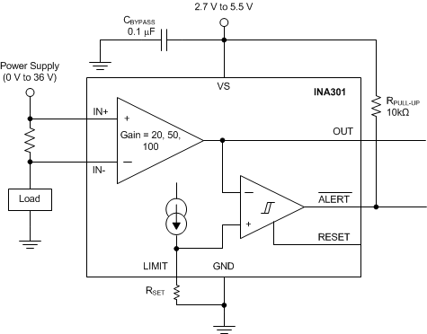
The INA301 is a 36-V common-mode, zero-drift topology, current-sensing amplifier that can be used in both low-side and high-side configurations. These specially-designed, current-sensing amplifiers are able to accurately measure voltages developed across current-sensing resistors (also known as current-shunt resistors) on common-mode voltages that far exceed the supply voltage powering the device. Current can be measured on input voltage rails as high as 36 V, and the device can be powered from supply voltages as low as 2.7 V. The device can also withstand the full 36-V common-mode voltage at the input pins when the supply voltage is removed without causing damage.
The zero-drift topology enables high-precision measurements with maximum input offset voltages as low as 35 μV with a temperature contribution of only 0.5 μV/°C over the full temperature range of –40°C to +125°C. The low total offset voltage of the INA301 enables smaller current-sense resistor values to be used, and allows for a more efficient system operation without sacrificing measurement accuracy resulting from the smaller input signal.
The INA301 uses a single external resistor to allow for a simple method of setting the corresponding current threshold level for the device to use for out-of-range comparison. Combining the precision measurement of the current-sense amplifier and the on-board comparator enables an all-in-one overcurrent detection device. This combination creates a highly-accurate solution that is capable of fast detection of out-of-range conditions and allows the system to take corrective actions to prevent potential component or system-wide damage.
7.2 Functional Block Diagram
7.3 Feature Description
7.3.1 Alert Output
The device ALERT pin is an active-low, open-drain output that is designed to be pulled low when the input conditions are detected to be out-of-range. This open-drain output pin is recommended to include a 10-kΩ, pullup resistor to the supply voltage. This open-drain pin can be pulled up to a voltage beyond the supply voltage, VS, but must not exceed 5.5 V.
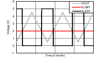
Figure 36 shows the alert output response of the internal comparator. When the output voltage of the amplifier is lower than the voltage developed at the LIMIT pin, the comparator output is in the default high state. When the amplifier output voltage exceeds the threshold voltage set at the LIMIT pin, the comparator output becomes active and pulls low. This active low output indicates that the measured signal at the amplifier input has exceeded the programmed threshold level, indicating an overcurrent or out-of-range condition has occurred.
7.3.2 Alert Mode
The device has two output operating modes, transparent and latched, that are selected based on the RESET pin setting. These modes change how the ALERT pin responds following an alert when the overcurrent condition is removed.
7.3.2.1 Transparent Output Mode
The device is set to transparent mode when the RESET pin is pulled low, thus allowing the output alert state to change and follow the input signal with respect to the programmed alert threshold. For example, when the differential input signal rises above the alert threshold, the alert output pin is pulled low. As soon as the differential input signal drops below the alert threshold, the output returns to the default high output state. A common implementation using the device in transparent mode is to connect the ALERT pin to a hardware interrupt input on a microcontroller. As soon as an overcurrent condition is detected and the ALERT pin is pulled low, the controller interrupt pin detects the output state change and can begin making changes to the system operation required to address the overcurrent condition. Under this configuration, the ALERT pin transition from high to low is captured by the microcontroller so the output can return to the default high state when the overcurrent event is removed.
7.3.2.2 Latch Output Mode
Some applications do not have the functionality available to continuously monitor the state of the output ALERT pin to detect an overcurrent condition as described in the Transparent Output Mode section. A typical example of this application is a system that is only able to poll the ALERT pin state periodically to determine if the system is functioning correctly. If the device is set to transparent mode in this type of application, the state change of the ALERT pin can be missed when ALERT is pulled low to indicate an out-of-range event if the out-of-range condition does not appear during one of these periodic polling events. Latch mode is specifically intended to accommodate these applications.
The device is placed into the corresponding output modes based on the signal connected to RESET, as shown in Table 1. The difference between latch mode and transparent mode is how the alert output responds when an overcurrent event ends. In transparent mode (RESET = low), when the differential input signal drops below the limit threshold level after the ALERT pin asserts because of an overcurrent event, the ALERT pin state returns to the default high setting to indicate that the overcurrent event has ended.
Table 1. Output Mode Settings
| OUTPUT MODE | RESET PIN SETTING |
|---|---|
| Transparent mode | RESET = low |
| Latch mode | RESET = high |
In latch mode (RESET = high), when an overlimit condition is detected and the ALERT pin is pulled low, the ALERT pin does not return to the default high state when the differential input signal drops below the alert threshold level. In order to clear the alert, the RESET pin must be pulled low for at least 100 ns. Pulling the RESET pin low allows the ALERT pin to return to the default high level provided that the differential input signal has dropped below the alert threshold. If the input signal is still above the threshold limit when the RESET pin is pulled low, the ALERT pin remains low. When the alert condition is detected by the system controller, the RESET pin can be set back to high in order to place the device back in latch mode.
The latch and transparent modes are represented in Figure 37. In Figure 37, when VIN drops back below the VLIMIT threshold for the first time, the RESET pin is pulled high. With the RESET pin is pulled high, the device is set to latch mode so that the alert output state does not return high when the input signal drops below the VLIMIT threshold. Only when the RESET pin is pulled low does the ALERT pin return to the default high level, thus indicating that the input signal is below the limit threshold. When the input signal drops below the limit threshold for the second time, the RESET pin is already pulled low. The device is set to transparent mode at this point and the ALERT pin is pulled back high as soon as the input signal drops below the alert threshold.
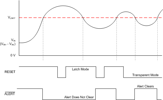 Figure 37. Transparent versus Latch Mode
7.3.3 Setting The Current-Limit Threshold
The INA301 determines if an overcurrent event is present by comparing the amplified measured voltage developed across the current-sensing resistor to the corresponding signal developed at the LIMIT pin. The threshold voltage for the LIMIT pin can be set using a single external resistor or by connecting an external voltage source to the LIMIT pin.
7.3.3.1 Resistor-Controlled Current Limit
The typical approach for setting the limit threshold voltage is to connect a resistor from the LIMIT pin to ground. The value of this resistor, RLIMIT, is chosen in order to create a corresponding voltage at the LIMIT pin equivalent to the output voltage, VOUT, when the maximum desired load current is flowing through the current-sensing resistor. An internal 80-µA current source is connected to the LIMIT pin to create a corresponding voltage used to compare to the amplifier output voltage, depending on the value of the RLIMIT resistor.
In the equations from Table 2, VTRIP represents the overcurrent threshold that the device is programmed to monitor for and VLIMIT is the programmed signal set to detect the VTRIP level.
Table 2. Calculating the Limit Threshold Setting Resistor, RLIMIT
| PARAMETER | EQUATION | |
|---|---|---|
| VTRIP | VOUT at the desired current trip value | ILOAD × RSENSE x Gain |
| VLIMIT | Threshold limit voltage | VLIMIT = VTRIP |
| ILIMIT × RLIMIT | ||
| RLIMIT | Calculate the threshold limit-setting resistor | VLIMIT / ILIMIT |
| VLIMIT / 80 µA | ||
7.3.3.1.1 Resistor-Controlled Current Limit: Example
For example, if the current level indicating an out-of-range condition is present is 20 A and the current-sense resistor value is 10 mΩ, then the input threshold signal is 200 mV. The INA301A1 has a gain of 20 so the resulting output voltage at the 20-A input condition is 4 V. The value for RLIMIT is selected to allow the device to detect to this 20-A threshold, indicating an overcurrent event has occurred. When the INA301 detects this out-of-range condition, the ALERT pin asserts and pulls low. For this example, the value of RLIMIT to detect a 4-V level is calculated to be 50 kΩ, as shown in Table 3.
Table 3. Calculating the Limit Threshold Setting Resistor, RLIMIT: Example
| PARAMETER | EQUATION | |
|---|---|---|
| VTRIP | VOUT at the desired current trip value | ILOAD × RSENSE x Gain |
| 20 A x 10 mΩ x 20 V/V = 4 V | ||
| VLIMIT | Threshold limit voltage | VLIMIT = VTRIP |
| ILIMIT × RLIMIT | ||
| RLIMIT | Calculate the threshold limit-setting resistor | VLIMIT / ILIMIT |
| 4 V / 80 µA = 50 kΩ | ||
7.3.3.2 Voltage-Source-Controlled Current Limit
The second method for setting the limit voltage is to connect the LIMIT pin to a programmable digital-to-analog converter (DAC) or other external voltage source. The benefit of this method is the ability to adjust the current-limit threshold to account for different threshold voltages that are used for different system operating conditions. For example, this method can be used in a system that has one current-limit threshold level that must be monitored during a power-up sequence but different threshold levels that must be monitored during other system operating modes.
In Table 4, VTRIP represents the overcurrent threshold that the device is programmed to monitor for and VSOURCE is the programmed signal set to detect the VTRIP level.
Table 4. Calculating the Limit Threshold Voltage Source, VSOURCE
| PARAMETER | EQUATION | |
|---|---|---|
| VTRIP | VOUT at the desired current trip value | ILOAD × RSENSE × Gain |
| VSOURCE | Program the threshold limit voltage | VSOURCE = VTRIP |
7.3.4 Selecting a Current-Sensing Resistor
The device measures the differential voltage developed across a resistor when current flows through the component to determine if the current being monitored exceeds a defined limit. This resistor is commonly referred to as a current-sensing resistor or a current-shunt resistor, with each term commonly used interchangeably. The flexible design of the device allows for measuring a wide differential input signal range across this current-sensing resistor.
Selecting the value of this current-sensing resistor is based primarily on two factors: the required accuracy of the current measurement and the allowable power dissipation across the current-sensing resistor. Larger voltages developed across this resistor allow for more accurate measurements to be made. Amplifiers have fixed internal errors that are largely dominated by the inherent input offset voltage. When the input signal decreases, these fixed internal amplifier errors become a larger portion of the measurement and increase the uncertainty in the measurement accuracy. When the input signal increases, the measurement uncertainty is reduced because the fixed errors are a smaller percentage of the signal being measured. Therefore, the use of larger value current-sensing resistors inherently improves the measurement accuracy.
However, a system design trade-off must be evaluated through use of larger input signals for improving the measurement accuracy. Increasing the current sense resistor value results in an increase in power dissipation across the current-sensing resistor. Increasing the value of the current-shunt resistor increases the differential voltage developed across the resistor when current passes through the component. This increase in voltage across the resistor increases the power that the resistor must be able to dissipate. Decreasing the value of the current-shunt resistor value reduces the power dissipation requirements of the resistor, but increases the measurement errors resulting from the decreased input signal. Selecting the optimal value for the shunt resistor requires factoring both the accuracy requirement for the specific application and the allowable power dissipation of this component.
An increasing number of very low ohmic-value resistors are becoming more widely available with values reaching down as low as 200 µΩ or lower with power dissipations of up to 5 W that enable large currents to be accurately monitored with sensing resistors.
7.3.4.1 Selecting a Current-Sensing Resistor: Example
In this example, the trade-offs involved in selecting a current-sensing resistor are discussed. This example requires 2.5% accuracy for detecting a 10-A overcurrent event where only 250 mW is allowable for the dissipation across the current-sensing resistor at the full-scale current level. Although the maximum power dissipation is defined as 250 mW, a lower dissipation is preferred to improve system efficiency. Some initial assumptions are made that are used in this example: the limit-setting resistor (RLIMIT) is a 1% component and the maximum tolerance specification for the internal threshold setting current source (0.5%) is used. Given the total error budget of 2.5%, up to 1% of error is available to be attributed to the measurement error of the device under these conditions.
As shown in Table 5, the maximum value calculated for the current-sensing resistor with these requirements is 2.5 mΩ. Although this value satisfies the maximum power dissipation requirement of 250 mW, headroom is available from the 2.5% maximum total overcurrent detection error to reduce the value of the current-sensing resistor and reduce the power dissipation further. Selecting a 1.5-mΩ, current-sensing resistor value offers a good tradeoff for reducing the power dissipation in this scenario by approximately 40% and still remaining within the accuracy region.
Table 5. Calculating the Current-Sensing Resistor, RSENSE
| PARAMETER | EQUATION | VALUE | UNIT | |
|---|---|---|---|---|
| IMAX | Maximum current | 10 | A | |
| PD_MAX | Maximum allowable power dissipation | 250 | mW | |
| RSENSE_MAX | Maximum allowable RSENSE | PD_MAX / IMAX2 | 2.5 | mΩ |
| VOS | Offset voltage | 150 | µV | |
| VOS_ERROR | Initial offset voltage error | (VOS / (RSENSE_MAX × IMAX ) × 100 | 0.6% | |
| EG | Gain error | 0.25% | ||
| ERRORTOTAL | Total measurement error | √(VOS_ERROR2 + EG2) | 0.65% | |
| Allowable current threshold accuracy | 2.5% | |||
| ERRORINITIAL | Initial threshold error | ILIMIT Tolerance + RLIMIT Tolerance | 1.5% | |
| ERRORAVAILABLE | Maximum allowable measurement error | Maximum Error – ERRORINITIAL | 1% | |
| VOS_ERROR_MAX | Maximum allowable offset error | √(ERRORAVAILABLE2 – EG2) | 0.97% | |
| VDIFF_MIN | Minimum differential voltage | VOS / VOS_ERROR_MAX (1%) | 15 | mV |
| RSENSE_MIN | Minimum sense resistor value | VDIFF_MIN / IMAX | 1.5 | mΩ |
| PD_MIN | Lowest possible power dissipation | RSENSE_MIN × IMAX2 | 150 | mW |
7.3.5 Hysteresis
The on-board comparator in the INA301 is designed to reduce the possibility of oscillations in the alert output when the measured signal level is near the overlimit threshold level because of noise. When the output voltage (VOUT) exceeds the voltage developed at the LIMIT pin, the ALERT pin is asserted and pulls low. The output voltage must drop below the LIMIT pin threshold voltage by the gain-dependent hysteresis level in order for the ALERT pin to de-assert and return to the nominal high state, as shown in Figure 38.
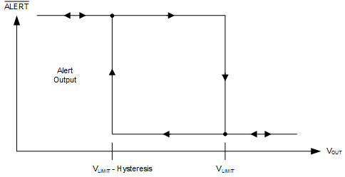 Figure 38. Typical Comparator Hysteresis
7.4 Device Functional Modes
7.4.1 Input Filtering
External system noise can significantly affect the ability of a comparator to accurately measure and detect whether input signals exceed the reference threshold levels, thus reliably indicating an overrange condition. The most obvious effect that external noise can have on the operation of a comparator is to cause a false alert condition. If a comparator detects a large noise transient coupled into the signal, the device can easily interpret this transient as an overrange condition.
External filtering can help reduce the amount of noise that reaches the comparator and reduce the likelihood of a false alert from occurring. The tradeoff to adding this noise filter is that the alert response time is increased because of the input signal being filtered as well as the noise. Figure 39 shows the implementation of an input filter for the device.
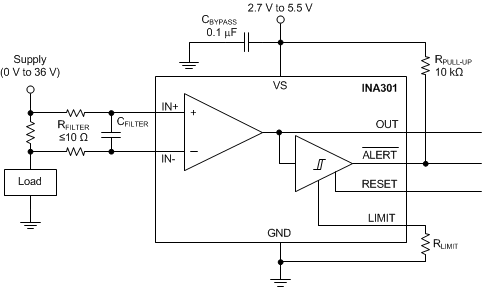 Figure 39. Input Filter
Limiting the amount of input resistance used in this filter is important because this resistance can have a significant affect on the input signal that reaches the device input pins resulting from the device input bias currents. A typical system implementation involves placing the current-sensing resistor very near the device so the traces are very short and the trace impedance is very small. This layout helps reduce the ability of coupling additional noise into the measurement. Under these conditions, the characteristics of the input bias currents have minimal affect on device performance.
As illustrated in Figure 40, the input bias currents increase in opposite directions when the differential input voltage increases. This increase results from the design of the device that allows common-mode input voltages to far exceed the device supply voltage range. With input filter resistors now placed in series with these unequal input bias currents, there are unequal voltage drops developed across these input resistors. The difference between these two drops appears as an added signal that (in this case) subtracts from the voltage developed across the current-sensing resistor, thus reducing the signal that reaches the device input pins. Smaller value input resistors reduce this effect of signal attenuation to allow for a more accurate measurement.
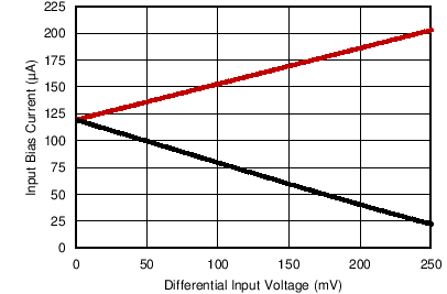
For example, with a differential voltage of 10 mV developed across a current-sensing resistor and using 20-Ω resistors, the differential signal that actually reaches the device is 9.85 mV. A measurement error of 1.5% is created as a result of these external input filter resistors. Using 10-Ω input filter resistors instead of the 20-Ω resistors reduces this added error from 1.5% down to 0.75%.
7.4.2 Using The INA301 with Common-Mode Transients Above 36 V
With a small amount of additional circuitry, the device can be used in circuits subject to transients higher than 36 V. Use only zener diodes or zener-type transient absorbers (sometimes referred to as transzorbs). Any other type of transient absorber has an unacceptable time delay. Start by adding a pair of resistors, as shown in Figure 41, as a working impedance for the zener diode. Keeping these resistors as small as possible is best, preferably 10 Ω or less. Larger values can be used with an additional induced error resulting from a reduced signal that actually reaches the device input pins. Because this circuit limits only short-term transients, many applications are satisfied with a 10-Ω resistor along with conventional zener diodes of the lowest power rating available. This combination uses the least amount of board space. These diodes can be found in packages as small as SOT-523 or SOD-523.
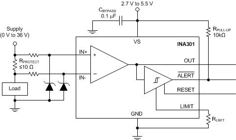 Figure 41. Transient Protection