SBOS775C
September 2016 – March 2019
INA302
,
INA303
PRODUCTION DATA.
1
Features
2
Applications
3
Description
Device Images
Typical Application
4
Revision History
5
Pin Configuration and Functions
Pin Functions
6
Specifications
6.1
Absolute Maximum Ratings
6.2
ESD Ratings
6.3
Recommended Operating Conditions
6.4
Thermal Information
6.5
Electrical Characteristics
6.6
Typical Characteristics
7
Detailed Description
7.1
Overview
7.2
Functional Block Diagram
7.3
Feature Description
7.3.1
Bidirectional Current Sensing
7.3.2
Out-of-Range Detection
7.3.3
Alert Outputs
7.3.3.1
Setting Alert Thresholds
7.3.3.1.1
Resistor-Controlled Current Limit
7.3.3.1.1.1
Resistor-Controlled Current Limit: Example
7.3.3.1.2
Voltage-Source-Controlled Current Limit
7.3.3.2
Hysteresis
7.4
Device Functional Modes
7.4.1
Alert Operating Modes
7.4.1.1
Transparent Output Mode
7.4.1.2
Latch Output Mode
8
Application and Implementation
8.1
Application Information
8.1.1
Selecting a Current-Sensing Resistor (RSENSE)
8.1.1.1
Selecting a Current-Sensing Resistor: Example
8.1.2
Input Filtering
8.1.3
Using the INA30x With Common-Mode Transients Greater Than 36 V
8.2
Typical Application
8.2.1
Design Requirements
8.2.2
Detailed Design Procedure
8.2.3
Application Curve
9
Power Supply Recommendations
10
Layout
10.1
Layout Guidelines
10.2
Layout Example
11
Device and Documentation Support
11.1
Documentation Support
11.1.1
Related Documentation
11.2
Related Links
11.3
Receiving Notification of Documentation Updates
11.4
Community Resources
11.5
Trademarks
11.6
Electrostatic Discharge Caution
11.7
Glossary
12
Mechanical, Packaging, and Orderable Information
Package Options
Mechanical Data (Package|Pins)
PW|14
MPDS360A
Thermal pad, mechanical data (Package|Pins)
Orderable Information
sbos775c_oa
sbos775c_pm
6.6
Typical Characteristics
at T
A
= 25°C, V
REF
= V
S
/ 2, V
SENSE
= 0 V, V
S
= 5 V, V
IN+
= 12 V, and
ALERT1
,
ALERT2
pullup resistors = 10 kΩ (unless otherwise noted)
Figure 1.
Input Offset Voltage Distribution (INA30xA1)
Figure 3.
Input Offset Voltage Distribution (INA30xA3)
Figure 5.
CMRR Distribution (INA30xA1)
Figure 7.
CMRR Distribution (INA30xA3)
Figure 9.
CMRR vs Frequency
Figure 11.
Gain Error Distribution (INA30xA2)
Figure 13.
Gain Error vs Temperature
Figure 15.
PSRR vs Frequency
V
S
= 5 V
Figure 17.
Input Bias Current vs Common-Mode Voltage
Figure 19.
Input Bias Current vs Temperature
Figure 21.
Quiescent Current vs Temperature
Figure 23.
0.1-Hz to 10-Hz Voltage Noise
(Referred to Input)
4-V
PP
output step
Figure 25.
Voltage Output Falling Step Response
Figure 27.
Start-Up Response
Figure 29.
LIMIT2 Current Source vs Temperature
Figure 31.
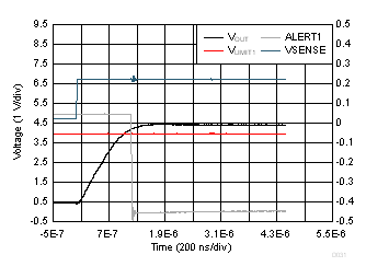
Comparator 1 Total Propagation Delay
(INA30x)
DELAY = 100 kΩ to V
S
Figure 33.
Comparator 2 Total Propagation Delay
(INA303)
DELAY = 100 kΩ to V
S
Figure 35.
Comparator 2 Total Propagation Delay
(INA302)
V
OD
= 1 mV
Figure 37.
Comparator 2 Propagation Delay vs Temperature
Figure 39.
Comparator 1 Hysteresis vs Temperature
Figure 41.
Comparator Latch Response
Figure 2.
Input Offset Voltage Distribution (INA30xA2)
Figure 4.
Input Offset Voltage vs Temperature
Figure 6.
CMRR Distribution (INA30xA2)
Figure 8.
CMRR vs Temperature
Figure 10.
Gain Error Distribution (INA30xA1)
Figure 12.
Gain Error Distribution (INA30xA3)
Figure 14.
Gain vs Frequency
Figure 16.
Output Voltage Swing vs Output Current
V
S
= 0 V
Figure 18.
Input Bias Current vs Common-Mode Voltage
Figure 20.
Quiescent Current vs Supply Voltage
Figure 22.
Input-Referred Voltage Noise vs Frequency
4-V
PP
output step
Figure 24.
Voltage Output Rising Step Response
Figure 26.
Common-Mode Voltage Transient Response
Figure 28.
LIMIT1 Current Source vs Temperature
Figure 30.
DELAY Current vs Temperature
DELAY = open
Figure 32.
Comparator 2 Total Propagation Delay
(INA303)
DELAY = open
Figure 34.
Comparator 2 Total Propagation Delay
(INA302)
V
OD
= 1 mV
Figure 36.
Comparator 1 Propagation Delay vs Temperature
Figure 38.
Comparator Alert V
OL
vs I
OL
Figure 40.
Comparator 2 Hysteresis vs Temperature